|
|
 |
A Stable 2m WSPR Transmit Beacon By: Bertrand Zauhar, VE2ZAZ
On this page, I describe my
implementation of a frequency-stable 1-Watt
144 MHz (2m band) WSPR Transmitter (Beacon)
based on QRP
Labs' Ultimate3S QRSS/WSPR kit. Using
the Ultimate3S for
2m WSPR is not possible unless a new
approach is taken to guarantee the frequency
stability required in WSPR transmission.
What follows is a detailed description of
what I did to make it operational, including
the design data, and the final solution so
that one can replicate the setup.
I was handed an assembled and functional Ultimate3S, with the objective of making it a 144 MHz WSPR beacon. A local amateur radio operator had previously tried to achieve this, but passed away before he could implement a solution. The Ultimate3S is a multi-mode self-contained HF QRP transmitter. It does a good job of transmitting WSPR data for propagation analysis. And the transmit frequency range includes the VHF 2m band, as long as proper output low pass filtering is implemented, obviously. Here are some important characteristics of a WSPR signal:
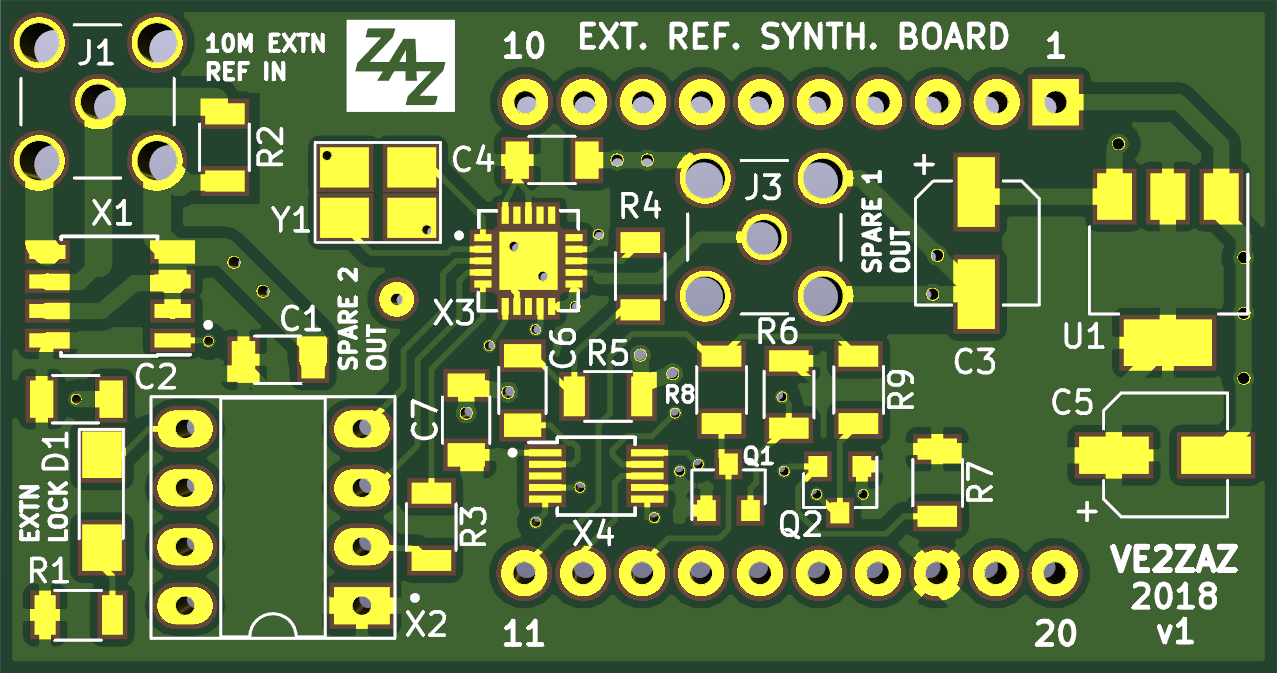
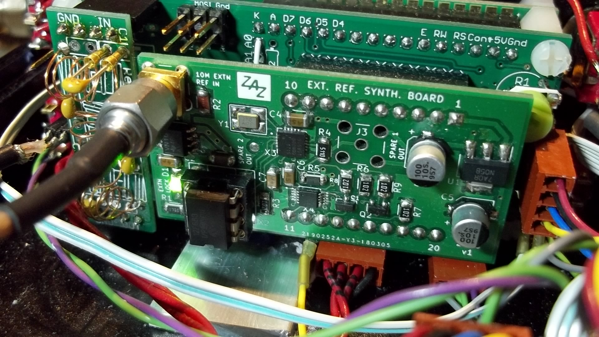
Consequently, I had to design my own 27.000 MHz frequency reference to be plug-in compatible with the existing OCXO design. That frequency, despite being rounded, is not a "standard" frequency on the market, and it is next to impossible to find an stabilized oscillator at that frequency. But 10.0000 MHz is a common standard frequency, and stable ovenized oscillators are readily available. The Silicon Laboratories Si5351 chip is a wonderful little beast for amateur radio. It is used everywhere in VFO and transmitter designs. Why not use an SI5351 as a frequency translator? 10.0000 MHz in, 27.0000 MHz out. Easy! But it has to be the C version of the chip, which has an external frequency reference input that can accept the 10 MHz reference. Some have used the A version (easier to solder leaded package) and brute-force 10 MHz into its 27 MHz crystal input. I do not like that solution, as it does not meet the chip's specs. The only real drawback of the SI5351C is that it is a lead-less, 4x4mm size QFN-20 package. Difficult to solder, but not impossible with a hot air rework station. To understand the proposed solution, the reader should become knowledgeable of Si5351 chip features, possibilities and limitations. This web page assumes so, and does not expand on those.
The best way to understand what the frequency reference translator board offers is by first consulting the Circuit Schematic of the board below (click on image to enlarge):  The circuit is rather
straightforward. The main features of this
printed circuit board are:
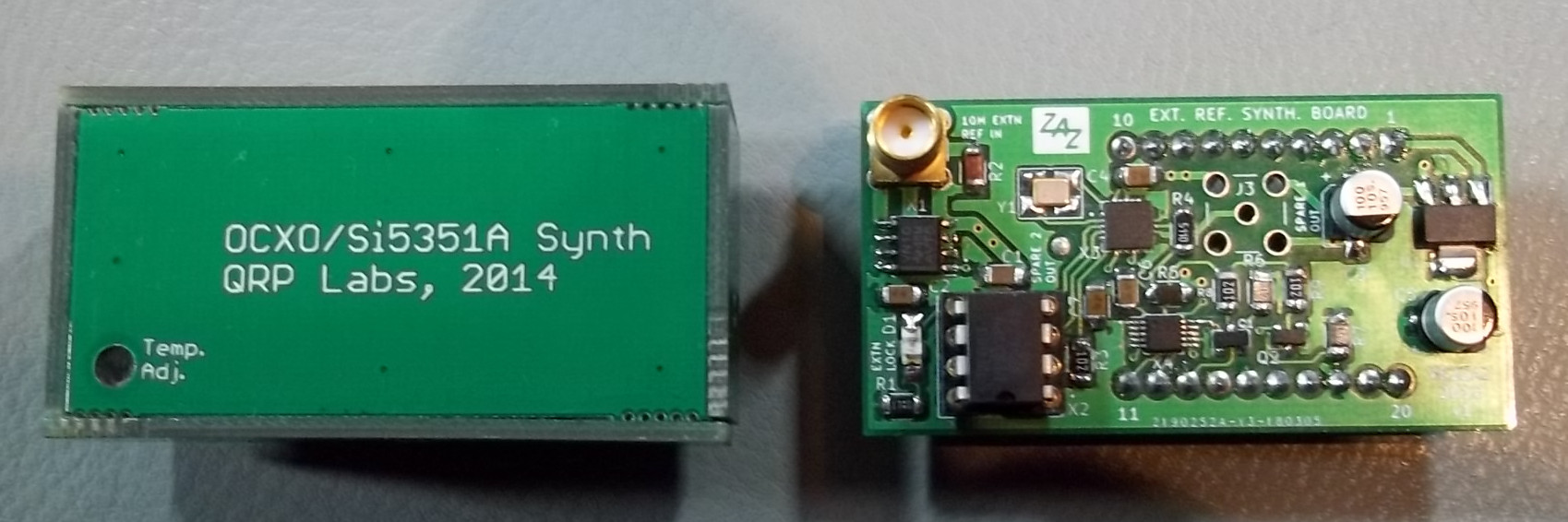
A side-by-side view of the QRP-Labs
27 MHz OCXO frequency reference (left),
and the VE2ZAZ Frequency Translator board (right). Both top and bottom sides are shown.
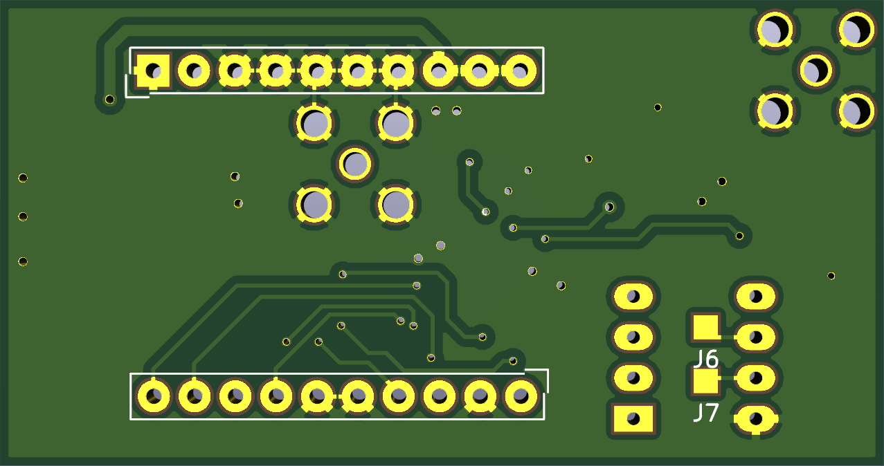
The Frequency Translator Printed Circuit Board is a double-sided design with plated-through holes, solder resist and silkscreen (marking). I provide the gerber and drill files for anyone who would like to replicate it. Such PCB can be ordered for around 20$ per lot of 10 PCBs. Simply provide the gerber files and the drill file to the manufacturer. I ordered from JLCPCB, but other manufacturers should produce the same quality. In your order, select 0.062" (1,6 mm) thickness FR-4 glass-epoxy material, the standard stuff.
The following is a list of all required components to put together this project. Some procurement recommendations are provided in the right hand side column. Other than the details provided, part selection is not critical.
One major challenge in assembling this board is the Si5351C soldering, which requires a hot-air rework station, some magnifying apparatus (camera or microscope), some soldering flux and a lot of skill. This is one VERY SMALL package! If you have never soldered this kind of device (QFN leadless), I recommend that you document yourself on the Internet prior to performing the work, or find someone who is willing to help with that task. This is an expensive chip, and you do not want to spoil it!
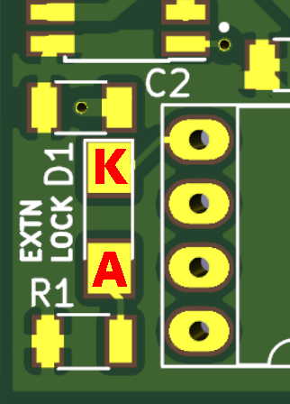
The Si5351A is also challenging, but to a lesser degree since it is a leaded package. The remaining of the board is not particularly difficult to assemble by hand if you can handle common surface-mounted components. A magnifying lamp, a fine tip soldering iron and a pair of tweezers are required. The lowest profile components should be installed first, starting with the Si-5351C chip, followed by theremaining surface-mounted components. Note that The electrolytic capacitors, the headers, the micro-controller dip socket and the SMA connectors should be installed last. The J4 and J5 headers must be installed on the PCB's bottom side, and soldered on the top side. Care should be put in properly orienting the LED during soldering. Read the LED documentation to figure out which electrode is the anode. See the image to the right on proper LED orientation on the PCB.
The PIC12F683 firmware (the program) was written in Microchip XC8 C v1.45 language and compiled in MPLAB X v5.30, both being downloadable free of charge. The code sets up the Si5351C for a 10 MHz input, translating into a 27 MHz output. Since there is no I2C peripheral on that PIC, the protocol is emulated in software, albeit at a much slower speed than the typical I2C bus. This does not cause any issue as this is a synchronous bus driven by the SCL clock signal. The calculated multiplier and PLL parameters are explained as comments in the "main.c" source file header. The source file also includes an optional configuration (currently commented out) for the spare output at 28.8000 MHz, a frequency commonly used to clock an RTL-SDR USB radio receiver. This could be useful to run an accompanying WSPR receiver. The .HEX file required for programming a PIC12F683 is located in the "dist/default/production" directory.
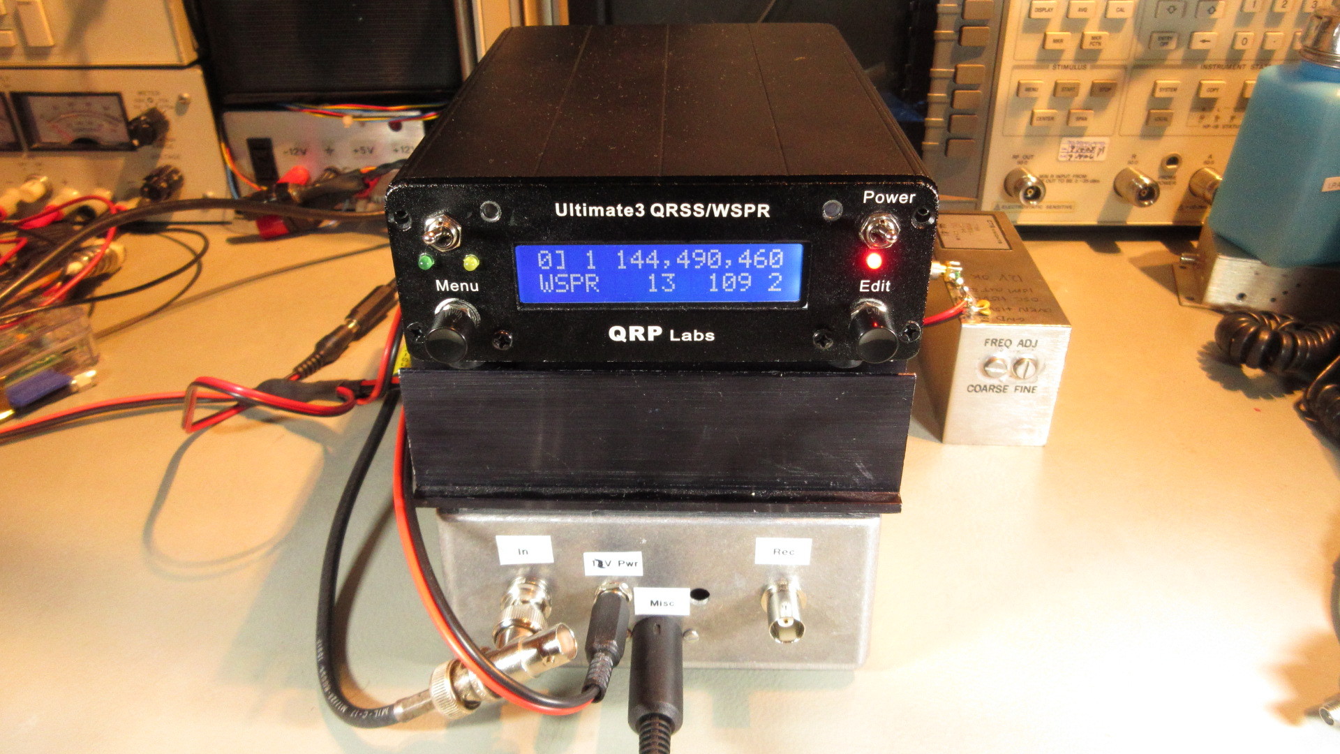
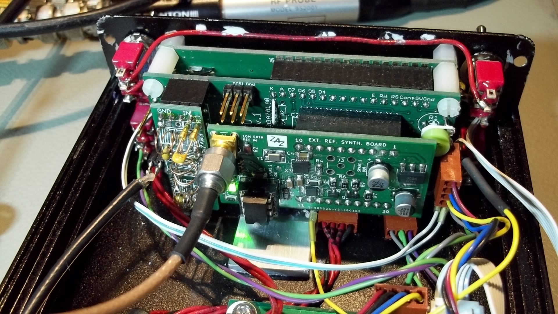
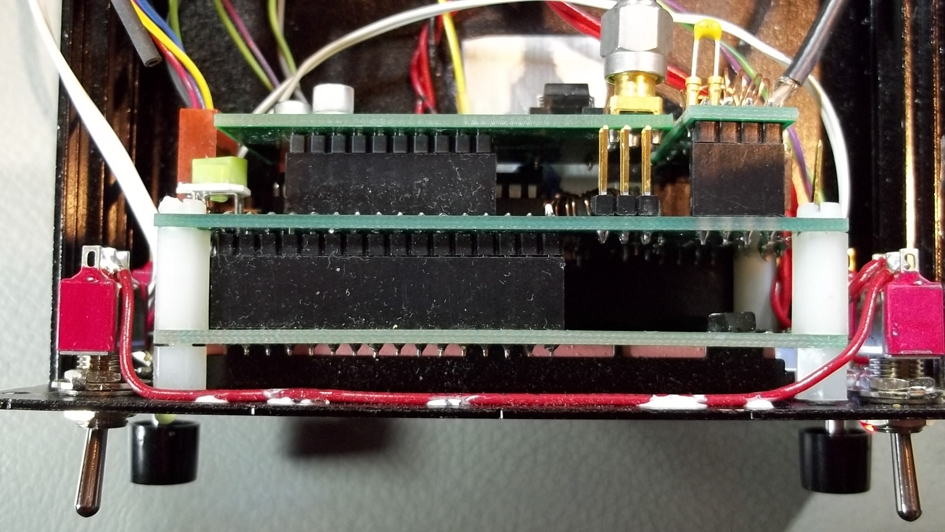
The final setup has three
stacked boards inside the Ultimate 3S,
namely the display board, the control
board and the VE2ZAZ reference translator
board. On the side is the plug-in
low-pass-filter module. The VE2ZAZ
reference translator board is plugged in
lieu of the
Si5351A Synthesizer module
kit or
the optional 27 MHz OCXO frequency
reference kit.
Other than the
external
reference
coaxial cable,
no other wiring
is needed. The
board is held
in place by the
header
connectors
friction.
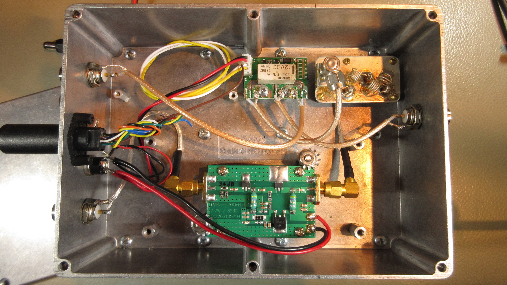
To boost the signal output from 100mW to 1W, I chose to use a pre-built Chinese-made 3.2W dual-stage broadband amplifier board. They are available everywhere on web sites such as eBay. These will run at a comfortable linear output of 1W. Notice that I have replaced the input attenuator on the amplifier board to get a 34 dB attenuation. The exact attenuation to get one Watt of RF output may vary from unit to unit, but do not send in the Ultimate3S output straight into the amplifier without proper attenuation! Also important, I have added a 2m 7-pole low-pass filter on the amplifier output to filter out undesired harmonics. In the box, I have also included a T/R relay board for future applications where receiving WSPR would be required.
Remember that the
output clock shape generated by
the Si5351 chip is a square wave.
One must include proper lowpass or
bandpass filtering if the output
is to be used in radio
applications, especially if it is to be used as a low
power transmitter connected
directly to an antenna!
This is the case here!
I have been running the 2m WSPR beacon continuously for more than a year without any issue whatsoever. And the amplifier is still running fine. Receptions reports are not pouring in, but hey, this is 2 meters! |