 An
RF-Sensing Alarm
An
RF-Sensing Alarm
Save your power amplifier stages...and your
reputation!
By
Bertrand Zauhar, VE2ZAZ
April 1998,
All Rights Reserved.
An
RF-Sensing Alarm
Save your power amplifier stages...and your
reputation!
By
Bertrand Zauhar, VE2ZAZ
April 1998,
All Rights Reserved.
Have you ever walked into your shack and found out that one of your transceivers was on the air? Surprise! That has happened to me twice in the last couple of years. Once, it was the packet TNC that had crashed, leaving the 2m transceiver on the air for I don't know how long. That obviously blocked the entire packet BBS traffic. Whoops! The second time, my 70cm satellite uplink transceiver and amplifier had been shooting 100W of RF at the stars for 30 minutes without my consent, thanks to one of the gizmos I had built to control the rig. Try to figure out how hot the linear was! I decided that I had enough of it. Another occurrence and I would jeopardize my reputation forever.
I had to build a device that would alert me when it detects a continuous RF transmission that lasts more than 5 minutes (a safe margin since I usually do not read the newspaper on the air!). The device would have to be broadband (HF/VHF/UHF), be sensitive enough to detect a 5W transmission from inside the shack using a telescopic antenna, and produce a sound loud enough to alert me anywhere in the house. It would also have to be self-contained, which means without any hookups to my radios. After a bit of reading and thinking, I came up with a solution that meets all the initial objectives. Here it is in detail.
Circuit description
The circuit shown in Figure 1 may look scary for some of you, but it is not. It can be broken down into four stages. Let's look at them one at a time.
Figure
1: Circuit Schematic (Click
on image to enlarge it)
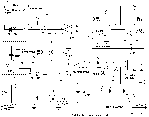
The first stage acts as a RF sensor circuit. It is made of U1C, one of the four operational amplifiers of a LM324 chip, and its associated input circuitry. U1C is used as a voltage comparator. Note that the two U1C inputs (plus and minus) have similar DC circuits connected to them. The plus input has R7, R8 and D3, and the minus input has R6, R10 and D5. In these two circuits, D3 and D4 are partly biased (about 200 mV of forward voltage) in order to better exploit the variation of voltage versus current that the diode produces. This translates into increased RF sensitivity.
In an idle condition (no RF detected), potentiometer R10 is set to make the voltage at the minus input of U1C slightly lower then the one at its plus input. This keeps the output of comparator U1C saturated to the "high" state (near supply V+). A strong RF signal present at the antenna terminal J1 reaches D3, a schottky diode, through C3, a coupling capacitor. The diode rectifies this signal and generates a drop of voltage at D3 anode. This makes the voltage at the plus input of U1C fall below the one set at the minus input. As a result, the output of comparator U1C flips down to the "low" state (near ground). In this state, the circuit is in RF detection mode and timer U1B is activated. Note that as soon as the RF signal disappears, the comparator immediately returns to its high state, resetting the entire alarm circuit. Ferrite bead FB1 and resistor R8 are used to block the RF from reaching comparator U1C. Additional RF decoupling is provided by capacitors C2 and C5.
The second stage acts as a timer. It is made of U1B, D4, C4 and R9. U1B is again used as a voltage comparator. When no RF is detected, capacitor C4 is kept charged by the "high" state of U1C. When RF is detected by the first stage, capacitor C4 is left "floating" and starts to slowly discharge through R9. When C4 is sufficiently discharged, after approximately 5 minutes, the voltage at the plus input of U1B falls below the one at the minus input which is set by D5 (about 200 mVDC). As a result, the output of comparator U1C flips down to the "low" state (near ground). In this state, the alarm is tripped. The timer stage drives piezo oscillator U1A and PNP transistor Q1. The latter is added to drive an external device with a voltage close to V+ when the alarm is tripped. The two diodes in series with the emitter provide a drop of voltage so that the base-emitter junction of Q1 is not biased when U1B output is in "high" state. The 2N3906 or equivalent transistor will safely supply a current of up to 50 mA.
The third stage is an astable multivibrator (square wave oscillator) and is made of U1A and surrounding components. It drives the piezo vibrator to produce a loud high-pitch sound. The oscillator circuit will operate only when the output of U1B presents a "low" state. Diode D2 serves as an isolating device between the two stages when U1B is in "low" state. The oscillator's frequency is set by capacitor C1 and resistor R5. The values chosen make the circuit oscillate at approximately 2600 Hz, a frequency that causes the piezo to generate the loudest sound.
The last stage is a simple buffer U1D that sinks current to turn on LED D1 whenever a RF signal is sensed by U1C. R1 limits the current to a safe level for the buffer, less than 20 mA.
The balanced input configuration of comparator U1C allows the supply voltage V+ to vary over a wide range and the entire circuit will still work. I designed the circuit for a 13.8 V supply, but I verified that the circuit works down to approximately 10 V without recalibrating it, and down to approximately 5 V if recalibrated. The high end of the range is more delicate to set since devices such as the LED, the piezo vibrator and polarized capacitors may be overstressed if component value changes are not made. Consequently, I would not recommend going beyond 20 V.
Circuit Assembly
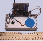
First, let me say that this project is relatively inexpensive to assemble. If all the components are purchased, it should cost less than $25 to build it. Obviously, your junkbox's size will dictate the cost. I re-used components taken from old PCBs. This allowed me to build the project for less than five dollars, including PCB and box.
Figure 2 shows the component layout and the double-sided PCB layout .
Figure
2: PCB Layout (Click on
image to enlarge it)
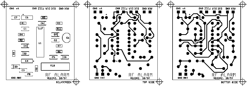
I admit, it is a rather compact design. The intent here is to make the design fit in a very common Hammond 1591A plastic box. Note that the circuit can be assembled using other techniques: universal PCB, veroboard, deadbug, wire-wrap and even a combination of these techniques. The layout is not critical except for the RF portion of the circuit: Components D3, C3, FB1 and R8 should be mounted as close of possible to each other using very short leads. This will guarantee proper operation up into the UHF spectrum. Also, decoupling capacitors C2 and C5 should be mounted as close as possible to pins 9 and 10 of U1C.
When assembling the PCB, use a soldering iron with a fine tip. Start by installing the LM324 IC. This is the hardest component to solder because of the pin spacing and overall PCB component density. An IC socket is desirable since the LM324 is rather sensitive to pin shorting compared to other operational amplifiers I've used in the past. With a socket, replacing it is a snap. Make sure you solder all components on the two PCB sides. Many component leads are used as vias to jump from top to bottom layers. Soldering all components this way guarantees you a functional circuit at the end. It's happened to me too often to forget to solder a component on the component side of the PCB.
Ferrite bead FB1 is inserted over a short piece of solid wire and the wire is soldered to the PCB pads. Potentiometer R10 is located on the PCB edge so that its adjustment screw can be accessed through a small hole drilled on one of the faces of the box. I've chosen not to put connectors for external connections to the LED, the piezo vibrator, supply line and the auxiliary output. Solder small gauge (#26 or smaller) wires directly to the PCB pads and connect the other ends to the external devices.
For antenna connection, I recommend using a female panel-mount BNC connector. It is small, reliable and will accept most right-angled telescopic antennas when mounted horizontally. Other RF connectors can be used if desired. Since the input impedance of the circuit is quite high, maintaining a constant impedance through the connectors is not an issue. In general though, it is good practice to avoid using UHF connectors (PL-259/SO-239) when working above 200 MHz, since they are not of constant impedance type. For coaxial cable, a short piece of RG-174 type or equivalent is preferred to limit overstressing of the PCB pads. This type of coax is much easier to route in a small box anyway. Solder the bare ends directly to the pads.
Someone may decide that 5 minutes of margin before alerting is too short. C4 and R9 make up the RC circuit that determines the duration. The discharge rate can be varied by changing the value of C4 and/or R9. Figure 3 shows a plot of resistor R9 as a function of time for different supply voltages V+.
Figure
3: R9 vs Time (Click on
image to enlarge it)
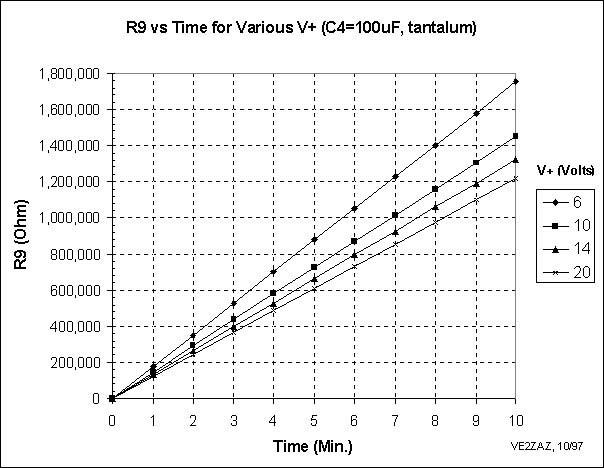
This graph gives a "ball park" idea of the resistor value to pick. I computed this graph using a tantalum capacitor for C4. I verified that, in general, tantalum capacitors match closer to the theoretical exponential discharge curve than do electrolytic capacitors. If an electrolytic capacitor is used instead, the user can expect to get about 10 % longer duration than what is indicated on the graph. Electrolytic capacitors are far from being perfect devices (farther than tantalum) and their "unwanted" characteristics tend to lengthen the discharge duration. Also note that tolerances on the capacitor values will affect the duration as well.
Here are some comments on the piezo vibrator. First, piezo vibrators have a "resonance" frequency that when submitted to, produces the loudest sound. The piezo I used came out of my junk box. I found that a 10K resistor for R5 produced the loudest, most unpleasant sound. Using a different piezo element may require a different value of resistance. I suggest temporarily connecting a 50 KOhm potentiometer to find your piezo's "sweet spot". You can then measure the required resistance with an ohmmeter directly on the potentiometer and substitute it with the closest resistor value at the end.
Second, you may have noticed that some piezo vibrators have three wires and some have two. Only two wires are used here. The third wire is a feedback signal. If the piezo you are using has three wires, the black wire goes to ground, the red goes to the oscillator and the blue (or other color) is not connected.
Third, make sure you use an "external drive" type of piezo vibrator. Some piezos come with built in oscillator circuits and will only function if they are connected to the auxiliary output provided by Q1.
Finally, if means of alerting other than piezo are preferred, you can use the auxiliary output to drive an external device. In this case you don't have to install components R1, R2, R4, R5, C1 and D2. Put jumper leads at the place of C1 and R4 to ground the unused LM324 inputs.
Calibrating and Testing
When everything is assembled and visually inspected, it is time to apply DC supply to the circuit. When doing so, if the piezo sounds right away, adjust R10 until it stops. If you can monitor the supply current to the design using an ammeter, it should be less than 10 mA. Next do the touching test. There should not be any hot components.
Diodes D3 and D5 must be at the same temperature before calibration is performed. This is critical since temperature offsets can create milliVolts of difference and unbalance the circuit. So do not touch the PCB for a few minutes before going any further. To calibrate the unit you will need a digital voltmeter of 10 MOhm or higher input impedance that can read down to the milliVolt. First connect the voltmeter between U1C pin 10 and ground. Measure the voltage and note it down. Then move the voltmeter's red probe to U1C pin 9. Adjust potentiometer R10 to bring the voltage at pin 9 higher than the voltage previously measured at pin 10. The LED should turn on. Backing off on R10 to bring the voltage below the one at pin 10 should turn off the LED. This verifies that the Comparator stage is working properly. Now, adjust potentiometer R10 so that the voltmeter reading on pin 9 is 3 to 5 mV lower that the value noted from pin 10. This completes calibration.
At this point you are ready to verify the circuit using RF. Attach an antenna to J1. Transmit a constant amplitude signal (AM, FM, modulated SSB) from any of your radios with at least 5W of output power (using another antenna, of course!) and verify that the LED comes on when RF is present. Moving the antenna around in the shack, for example close to a window, may give better results. To verify the alarm circuit, you must maintain RF presence for at least 5 minutes before you can hear the sound. Make sure the frequency chosen will not interfere with ongoing QSOs and identify yourself often. When the alarm sounds, stop transmitting and verify that the alarm stops and that the LED turns off. Try detecting RF at other frequencies to verify sensitivity flatness.
Performance
Using a calibrated signal generator, I verified that the alarm's sensitivity is about 7 mV RMS of RF and is quite flat from 1MHz to 550MHz. Sensitivity depends on how close the two voltages at the inputs of comparator U1C are. The circuit is stable as long as the entire design is at the same temperature. This is the case when all the electronics are enclosed in a box. I've used the alarm for a few months now and haven't had to recalibrate it. Since the RF sensing circuit is not tuned, selectivity is dictated by the type of antenna used. I found that about 2 feet of antenna is enough for proper operation at all frequencies, HF, VHF, UHF. I put the alarm box on top of my radio console and I use a telescopic antenna (not selective...). Note also that my shack in located in a basement. A bit of experimenting here with antenna type, position and length may be required. I've also verified that I can hear the alarm sounding wherever I am located in the house. This sound is equivalent to a smoke detector, so you shouldn't have any problems hearing it.
Conclusion
I have not been alerted by my new alarm yet, but the day it happens I will be happy I had it. It gives me a peace of mind that I never had before. Are you going to wait until it happens to you before building this cool alarm? The choice is up to you...
Parts
List
| C1 | .01uF, ceramic |
| C2 | 1000pF, ceramic |
| C3 | 1000pF, ceramic |
| C5 | 1000pF, ceramic |
| C4 | 100uF, 25V, tantalum or electrolytic (see text) |
| C6 | 10uF, 25V tantalum or electrolytic |
| C7 | .1uF, ceramic |
| D1 | LED, any color |
| D2 | 1N4148 or equiv. |
| D3 | 1N5711, schottky |
| D4 | 1N4148 or equiv. |
| D5 | 1N5711, schottky |
| D6 | 1N4148 or equiv. |
| D7 | 1N4148 or equiv. |
| FB1 | Ferrite bead |
| J1 | BNC, Female panel mount |
| Q1 | 2N3906, PNP or equiv. |
| R1 | 100K |
| R2 | 100K |
| R4 | 100K |
| R3 | 1K |
| R5 | 10K |
| R6 | 1M |
| R7 | 1M |
| R8 | 27k |
| R9 | 470K |
| R10 | 50K, 10-turn pot., Bourns 3006 type |
| R11 | 22K |
| U1 | LM324 Quad Op. Amp. |
| X1 | Piezo, muRata PKM-11
or Radio Shack 273-73
or equiv. External drive type. |
| Socket | 14-pin DIP |
| Coax | Short piece of RG-174 or equiv. |
| Box | Hammond 1591A suggested |
| Ant | Right-angle BNC, telescopic |
Note: All resistors are 1/4 Watt, 5% tolerance