|

|
|
Stability
and
Accuracy
Improvements
to
the
HP 3586A/B/C Selective Level Meter SSB Audio
By:
Bertrand
Zauhar, VE2ZAZ
Page last
updated: 22/04/2011
This
page presents a modification to the Hewlett-Packard 3586A/B/C SLM
(receiver) BFO circuit that makes the entire SLM referenced to the
10MHz source, whether internal or external. This removes any SLM
receiver drift due to temperature. After the mod is performed, any
drift detected while making SSB audio tone
measurements external to the unit will not have the SLM drift embedded
into the measurements.
Good for FMT measurements! A
few hours of work and $25 or so will put you and keep you on frequency.
The HP 3586
Selective Level Meter (SLM)
is a great piece of test
equipment. It is a super HF receiver with lots of measurement bells and
wistles. One drawback of this equipment though is the fact that one of the mixing stage
LOs
is not derived from the on-board or externally fed 10MHz reference. The
last stage, the product detector has its BFOs (LSB, USB) free running
using regular quartz crystals. Unfortunately these drift. The drift is
insignificant and non-perceivable if you only listen to the SSB audio.
But if you perform long term tone frequency measurements, this is a
show stopper.
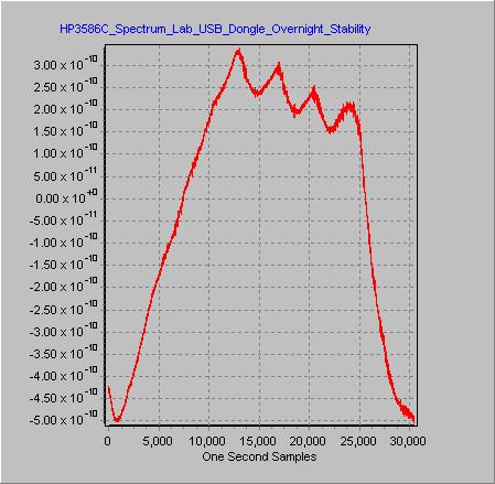
The plot below shows how much SSB BFO drift I detected using a stable
carrier fed into the RF input of the SLM. The audio tone produced by
the carrier was measured on a PC sound card using Spectrum Lab
software. This drift was caused by day-night-day variations in room
temperature. This was induced by a variation of around 2 degrees
Celcius. You can actually see the house heating system's behavior, with
a major night time reduction of temperature, a few heating cycles
overnight and a temperature recovery phase in the morning. Note that
the sound card drift was also measured, but it can be ruled out as a
major contributor in this plot since it drifts in the opposite
direction as a function of temperature.
So how
to improve this great test instrument and make it rock-solid? Here is
what I did.
The HP 3586 SLM uses two or three SSB LO frequencies internally,
depending on the model. They are the USB, LSB and Calibration
Mode frequencies. These frequencies vary as a function of the unit
model and
the equipped options. Here is a table extracted from the Service manual
that summarizes the various configurations:
HP 3586 Single
Sideband (SSB) L0 Frequencies.
|
| Model |
Opt. 003 |
Cal Active |
Bandwidth |
Sideband |
Crystal |
Crystal Freq. |
SSB L0 Freq. |
| 3586A/B |
YES |
NO |
3100Hz |
USB |
A22Y102 |
1.7475MHz |
17.475kHz |
| 3586A/B |
YES |
NO |
3100Hz |
LSB |
A22Y101 |
1.3775MHz |
13.775kHz |
| 3586A |
YES |
YES |
3100Hz |
- |
A7OY1 |
1.6425MHz |
16.425kHz |
| 3586B |
YES |
YES |
3100Hz |
- |
A7OY1 |
1.6625MHz |
16.625kHz |
| 3586A |
NO |
NO |
1740Hz |
USB |
A22Y102 |
1.6975MHz |
16.975kHz |
| 3586A |
NO |
NO |
1740Hz |
LSB |
A22Y101 |
1.4275MHz |
14.275kHz |
| 3586B |
NO |
NO |
2000Hz |
USB |
A22Y102 |
1.7125MHz |
17.125kHz |
| 3586B |
NO |
NO |
2000Hz |
LSB |
A22Y101 |
1.4125MHz |
14.125kHz |
| 3586C |
- |
NO |
3100Hz |
USB |
A22Y102 |
1.7475MHz |
17.475kHz |
| 3586C |
- |
NO |
3100Hz |
LSB |
A22Y101 |
1.3775MHz |
13.775kHz |
So the proposed solution has to be
reconfigurable on-the-fly, as the SSB mode is selected by the user via
the front panel pushbuttons and
when the Calibration state is invoked by the unit's firmware. It also
has to be flexible enough to accomodate the various SLM versions.
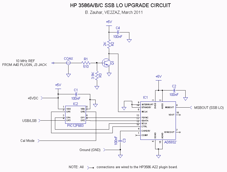
The Analog Devices AD5932
is a great little chip. It is a DDS-based Programmable Frequency
Waveform
Generator fitted inside a TSSOP 16-pin package. This chip has a
frequency divider with 224 steps. This means you can put out a
clock with a division resolution of 224 steps applied to the input reference
clock. What you also need is an accompanying chip to load the AD5932
with the right configuration at power up or when the SLM SSB mode is
changed. An 8-pin PIC12F683 is perfectly suited for this task.
Except
for the 10MHz clock reference, all
input and output signals to the proposed circuit are 5V-TTL logic, so
this is
a simple interface to the HP 3586, with a 5 VDC supply applied to both
the AD5932
and
the
PIC
micro.
The
10MHz
reference
signal
needs
a
bit
of
waveform
amplitude
and offset
scaling to make it a TTL-compatible clock; that can be perfromed by a
single NPN
transistor. Both chips and the transistor fit on a small add-on PCB that connects to
various points within the SLM.
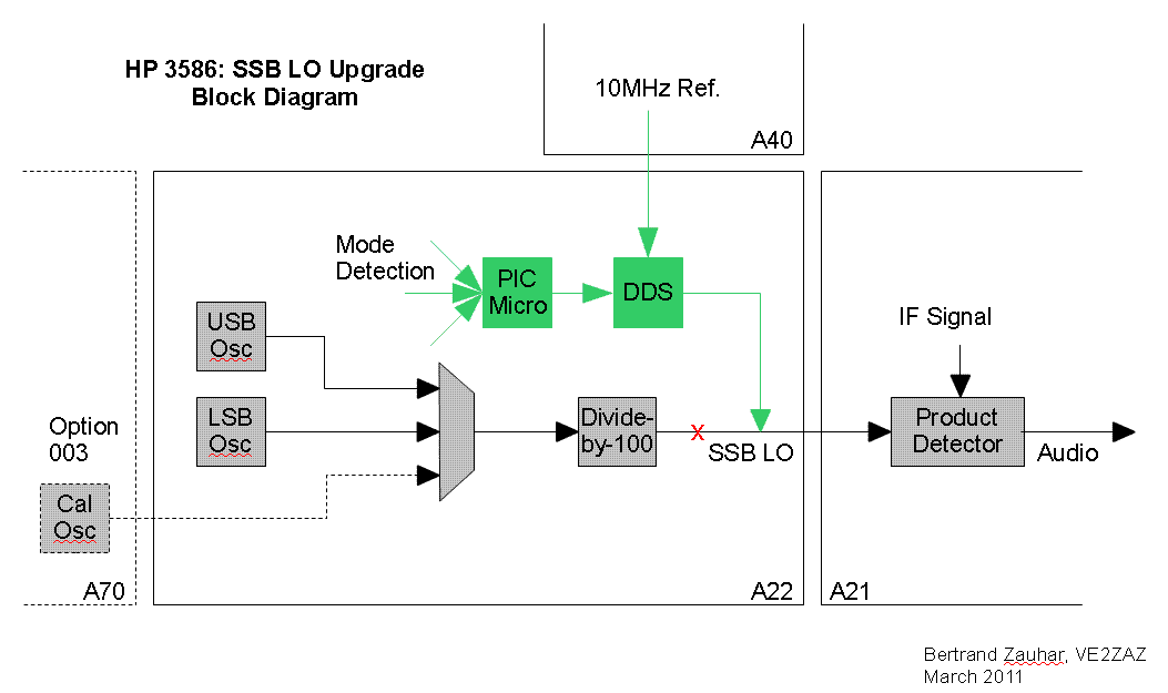
Here is a block
diagram that shows how this solution is implemented inside the HP 3586
SLM.
Here is a schematic
diagram of the proposed add-on circuit. Click
on the figure to see it in full size.
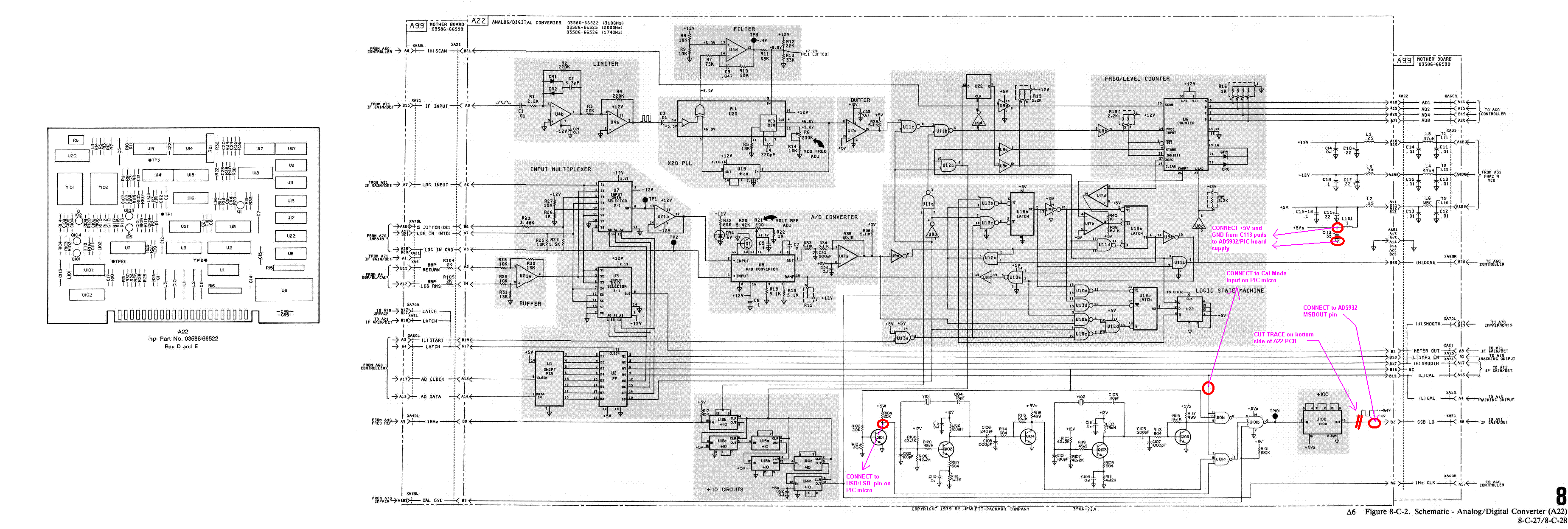
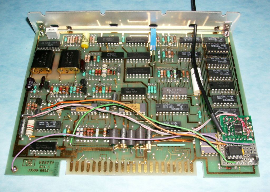
Inside
the HP 3586 SLM, almost all connections are made to module
A22, one of the plugins inside the unit. Here is a schematic page
extracted from the HP 3586 Service Manual that shows the required
hookups of the above circuit to
module A22. The annotations in red and pink are all there is to it as
far as the SLM itself. Click
on the figure to see it in full size.
The diagram above
also shows the A22 board layout on the left hand side, which will be
helpful to perform these
mods.
I have elected to
extract the 10MHz reference signal that drives the DDS chip directly
from the A40 plugin (the reference plugin) 10MHz output port normally
connected to the rear panel. In my case I don't need the 10MHz output
signal since my SLM does not have the OCXO option.
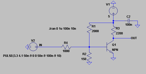
There are other locations within the SLM where a 10MHz reference could
be tapped off. These other points all use the PECL logic technology.
Consequently, a re-configuration of the 10MHz transistor circuit would
be required. Though I have not tried it, the following circuit would be
a better alternative when dealing with PECL logic swing since it has a
smaller swing. This is essentially a gain stage, with a gain of -5. Consider this circuit as just a
starting point; you may have to tweak the resistor values to center the
DC bias to the PN junction operating range.
I would appreciate
hearing from those who try the PECL avenue. I could update this page
with the information.
Note that
this upgrade
to the SLM has no impact to the built-in frequency and amplitude
measurement capabilities and specifications. This mod only affects the
product detector and the resulting SSB audio.
|
PERFORMING THE A22
PLUGIN PREPARATION WIRING
|
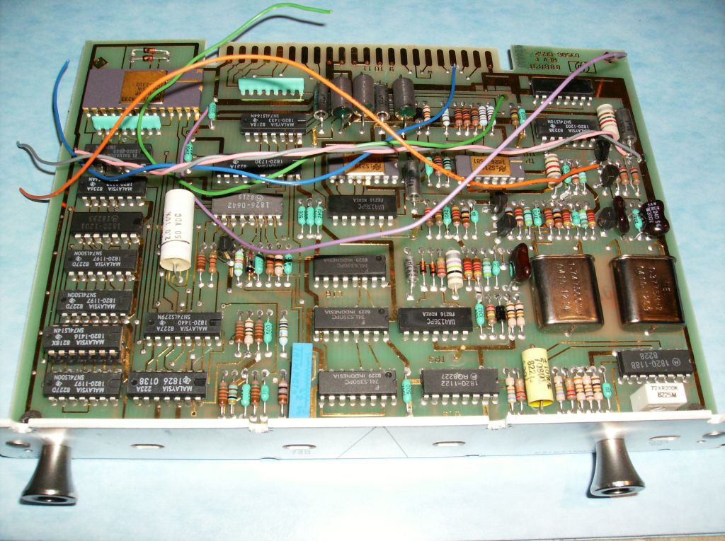
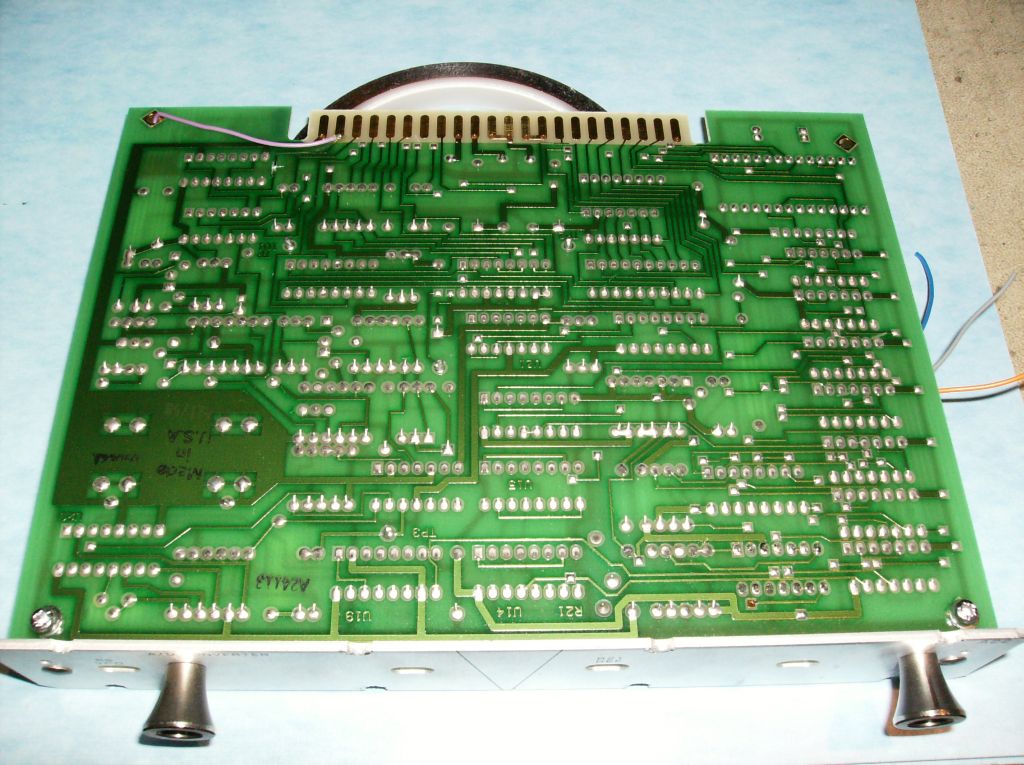
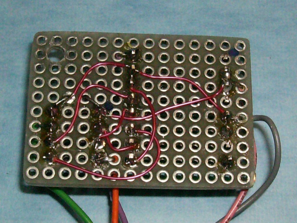
Here are two
pictures showing the wiring work required in preparation for receiving
the add-on board on the A22 plugin. Click
on the figure to see it in full size.
The following are a few instructions and notes that should be taken
into account when performing the mods on the HP 3586 A22 plugin card.
- One the picture above, please disregard the
blue wire. This was added for previous experimentation of this circuit
and is not required anymore.
- Working form the top of the 3586
unit, cover removed, you must remove the eight screws on the A22
faceplate, then pull out the plugin using the two knobs.
- All
added
wires
but
one
are
soldered
to
the
component side of A22.
- The
Axx row of card edge fingers is on the component side of the plugin
PCB, the Bxx row is on the solder side.
- On the solder side of the A22 plugin,
perform a cut on the trace that connects to card edge
finger B2. Use a sharp exacto knife. See solder side picture above
(upper-left corner).
- Again
seen on the solder side picture above, the purple wire is the MSBOUT
signal and it must be soldered to the solder side of the PCB,
and routed to the component side through the nearby hole. That wire may be
connected to card edge finger B2 or to the trace downstream from the
trace cut and toward card edge finger B2. If connecting to the
finger, make
sure you solder the wire to the very edge of
the finger, keeping in mind that the fingers get inserted into the A22
motherboard edge connector. I used kapton tape to keep the liquid
solder from envading the entire finger and contaminate the gold
plating. Refer to the picture above. If connecting to the trace,
you will have to scrape
off the solger resist to expose some copper.
- The
Cal Mode signal, shown as a green wire on the picture above, is only
used on the Option-003-equipped SLMs. Disregard otherwise and leave
unconnected on the PIC.
- This
Cal Mode signal can be
connected to the trace via hole shown in the picture. Follow the trace
from the card edge
finger B15 (solder side) to locate the via hole where to solder to on
the component side.
Note: It appears that there exists a
second version of the A22
board. There are major omponent differences and the board does
not look the same when comparing to the pictures above. Though I have
not seen a board of that other version, there is another version of HP
3586 circuit schematics that details it. If you happen to have one of
these different A22 boards, please communicate to me the changes you had to make to adapt my
mod to the other A22 board version. I will update this web page. Thanks.
|
ASSEMBLING
AND
MOUNTING
THE
ADD-ON
BOARD
ON
A22
|
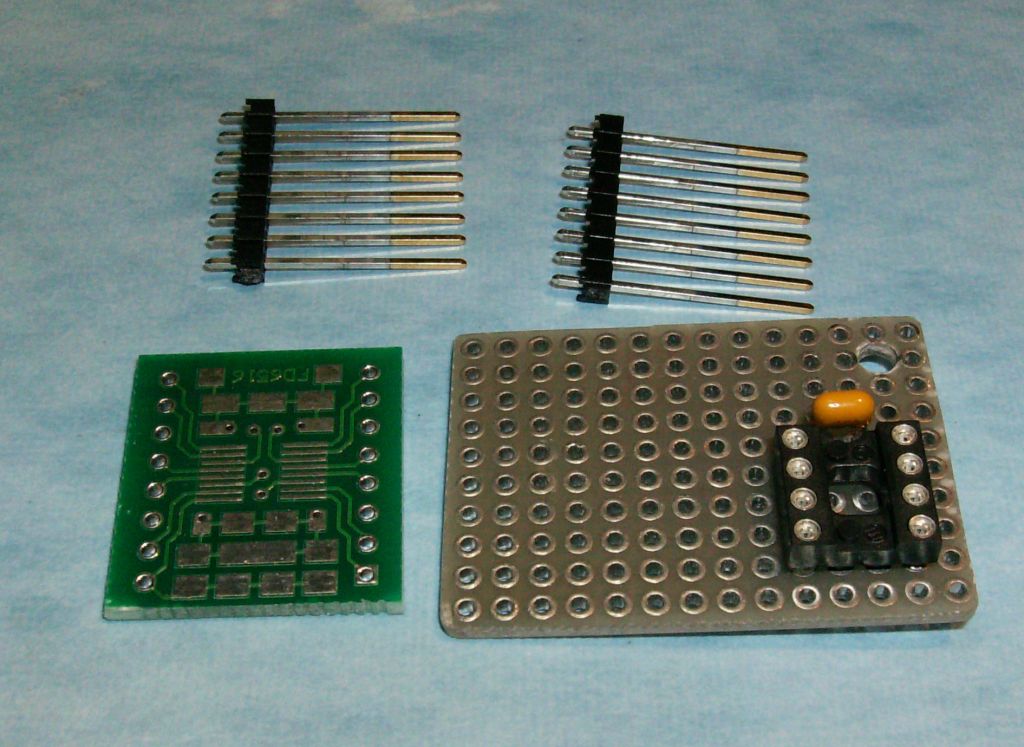
For this stage, there is more than one
option; mine is one suggestion, but you may adapt it based on the
availability of the PCB material or your junk box.
My add-on board is made of two PCBs, a prototype PCB and the TSSOP chip
carrier PCB. The former is a piece of plated-through prototype PCB. The
latter is a ready-made adapter board I purchased on eBay for a few
dollars. Searching for "SSOP DIP adapter" on eBay will yield several
solutions. Hobby electronics components websites are also a good place
to look for these.
Here are a few pictures showing how I put the add-on board together.
My TSSOP carrier PCB has extra pads to
install additional discrete components. With a bit of
planning, I could place all surface-mounted resistors, capacitors and
the transistor on
the TSSOP carrier PCB.
- I used parts of a 0.1 inch header strip
to mount/connect the TSSOP carrier PCB to the prototype PCB. I
suggest
you
first
solder
the
AD5932
chip
onto
the
carrier
PCB before soldering the header pins and the
other components. This gives
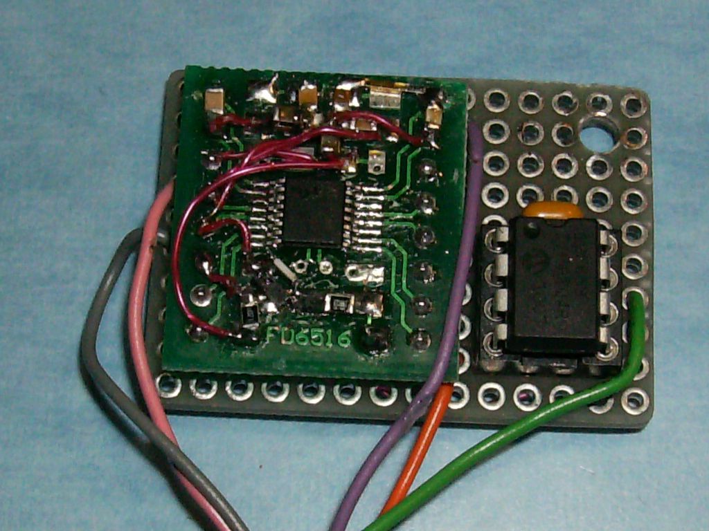
access from all angles for the soldering procedure.
- Soldering the AD5932 chip to the
carrier PCB is not an easy task and it requires skill, steady hands and
the right soldering iron, using the finest tip there is. Hot air
soldering is also possible if the pads are pre-tinned or if using
solder paste. In all cases, use liquid rosin flux to help the soldering
process. A good microscope or stereoscope is mandatory; a magnifying
lamp is not enough unfortunately. If you have not done this in the
past, ask a friend who has done it before for help. It may also be the
right time for you to consider upgrading your soldering/re-work tools...
- I used
(AWG-30 size) wire-wrap wire for the interconnects between the chips. I
strip both ends of their insulation and solder the wires to the pins.
- On
the
A22
plugin, I used the remaining corner mounting hole to install a
standoff post. I mounted the add-on board to the standoff. It keeps it
in a fixed location, away from the A22 components. Make sure that the
final assembly will fit back into the A22 compartment without causing
any short circuit. Notice that there are a few components mounted on
the motherboard inside the A22 compartment. The positioninng and size
of the final add-on board has to clear these components once the A22
plugin is fully inserted.
- Make
sure
there is not too much air
flow restriction as a result of the add-on board presence. The cooling
air is forced from the bottom of the SLM into the A22 compartment
through a few holes in the motherboard.
Here
is a picture of
the completed modification to the A22 plugin.
|
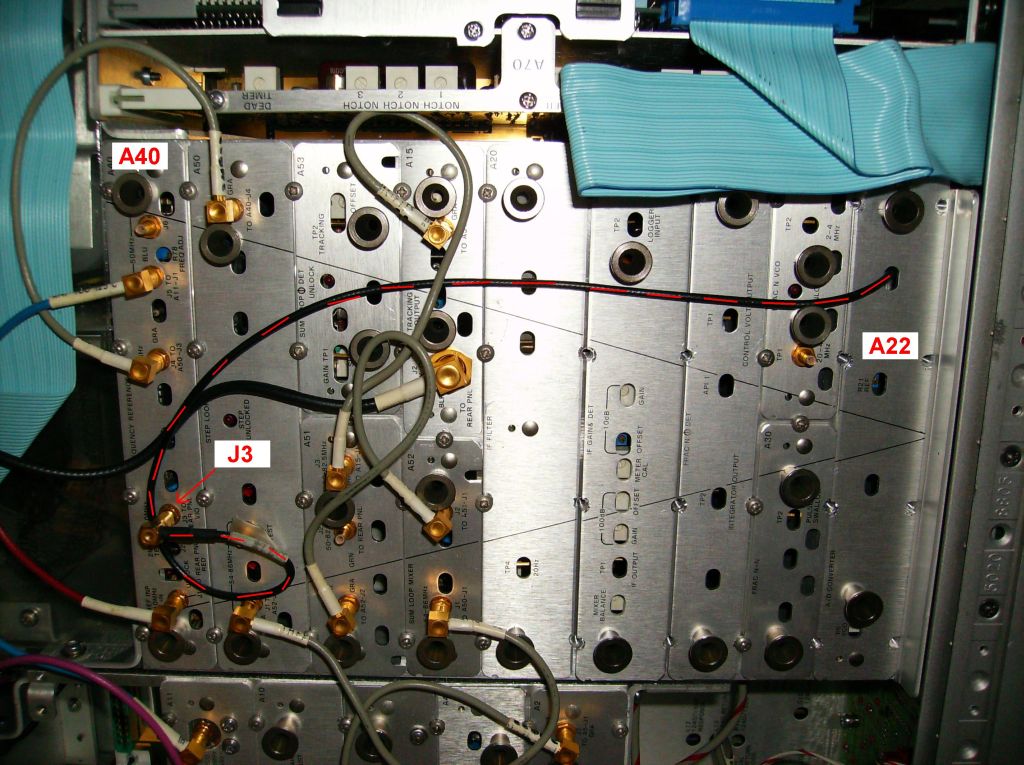
CONNECTING UP THE
10MHz REFERENCE
|
- Disconnect the
SMB coaxial cable
from port J3 on the A40 plugin faceplate. Connect a new coaxial cable
with a SMB connector at one end to J3.
- Route the new
cable towards the A22 plugin.
- Pass the cable
through one of
the ventilation holes on the A22 faceplate.
- Solder the coax
center
conductor to the transistor circuit on the add-on board. Leave the
shield unconnected at that end. Make sure the shield will not come in
contact with anything. I used heat shrink tubing to cover the exposed
shield.
The completed coaxial
connection is shown on the picture below.
I wrote the
source code in BoostC,
an
ANSI
C
compatible
language.
This
compiles
within
the
SourceBoost
IDE, a free programming environment. The Hex files required for
programming the PIC12F683 for the
various HP 3586 versions are also provided below.
Operation
After the modifications are performed and everything is assembled back
together, power up the unit. The SLM behavior should be exactly the
same as before when it performs its power up self-tests and when you
listen to radio signals. Use your best frequency
measurement technique to verify that the unit is right on expected
frequency and
that it does not drift as a function of temperature.
Again, this upgrade to the SLM has no impact to the built in frequency
and amplitude measurement capabilities. This mod only affects the
product detector, so the speaker audio and rear jack demodulated audio.
Stability
the main intent of this mod is to stabilize the SLM. The following plot
shows the drift of my HP 3586B before and
after the modification was applied. The heat up technique involves
blowing hot air into the rear air inlet (fan intake) for 30 seconds,
using a heat gun (paint stripper). The results speak for themselves...
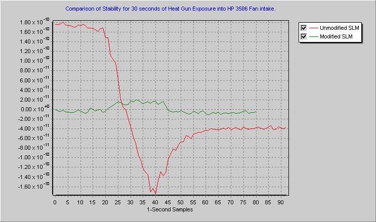
Note:
the
small
step
on
the
green
curve
detected
during heat gun action is
unlikely temperature related. This could be an effect generated by the
heat gun motor brushes. The heat gun stood right next to the audio
cable going to the sound card.
Accuracy
The table below shows the delta in Hz - Targeted
vs.Resulting - after the modification is performed to the SLM. This
is the closest that the AD5932 can produce to the intended frequencies
with a 10MHz reference as the MCLK signal.
As can be seen, the delta is less than 0.3 Hz from any targeted LO
frequency. This same absolute delta in Hertz is applied to
any detected RF signal. So a 10.000MHz received radio signal would
have a detected audio frequency error of better than 3x10⁻⁸
or 0.03 ppm, assuming a LO
delta of better than 0.3 Hz. Actual error can be computed by doing
Error_Hz / RxFreq_Hz, using the delta numbers below. Since these are
known fixed deltas in frequency, this can be used to compute the exact
frequency of any audio tone or received RF carrier.
HP 3586 Single
Sideband (SSB) L0 Frequencies: Targeted and Resulting
|
| Model |
Opt. 003 |
Cal Active |
Sideband |
Targeted L0 Freq |
Resulting LO Freq
|
Freq Delta |
| 3586A/B |
YES |
NO |
USB |
17475Hz |
17474.88976Hz |
-0.11024Hz
|
| 3586A/B |
YES |
NO |
LSB |
13775Hz |
13775.22945Hz |
0.22945Hz |
| 3586A |
YES |
YES |
- |
16425Hz |
16425.25196Hz
|
0.25196Hz |
| 3586B |
YES |
YES |
- |
16625Hz |
16624.92752Hz |
-0.07248Hz |
| 3586A |
NO |
NO |
USB |
16975Hz |
16974.80679Hz |
-0.19321Hz
|
| 3586A |
NO |
NO |
LSB |
14275Hz |
14274.71638Hz |
-0.28362Hz |
| 3586B |
NO |
NO |
USB |
17125Hz |
17125.01049Hz |
0.01049Hz |
| 3586B |
NO |
NO |
LSB |
14125Hz |
14125.10872Hz |
0.10872Hz |
| 3586C |
- |
NO |
USB |
17475Hz |
17474.88976Hz |
-0.11024Hz |
| 3586C |
- |
NO |
LSB |
13775Hz |
13775.22945Hz |
0.22945Hz |
In the process of
developing this solution, I have learned a lot on DDS technology. This
was an iterative development. The following is a series of comments
that will explain why the final solution looks like this.
- Initially,
the
intent
was
to
use
the
MSBOUT
(Most
Significant
Bit) output pin as
the LO source. This would have been great since the output is
TTL-leveled, exactly what the SLM phase detector is designed to work
with. Unfortunately, this MSBOUT signal is not a clean square wave.
There is some phase jitter produced by the DDS engine every few
milliseconds, stretching the pulse repeatedly. This produced some
modulated noise on the audio. Rejected.
- So I switched to the sine wave
output. That output does not have the TTL amplitude swing provided to
the product detector by the original circuit. Analyzing the product
detector stage on the A21 plugin revealed that the 500mV
pk-pk max swing from the AD5932 VOUT would be sufficient to drive the
MC1496 product detector chip, as long as the
voltage dividing resistor on its LO input is bypassed.
So
a
small
jumper
wire
on
resistor R5 of A21 would be required.
- I was to run the DDS with a 100KHz TTL signal for the MCLK.
I obviously did not grasp much of the DDS theory. I tried this but the
output waveform was very distorted, with 6 (roughly 100/16.5) steps per
tone cycle. Very ugly and almost impossible to filter to a clean sine
wave. The sound was terrible. Rejected.
- I switched to a 1
MHz TTL signal for the MCLK, which is available right on A22. Though
the SSB audio performance had drastically improved with more than 60
steps per tone cycle, there were still audible spur
tones.
Since
these
were
within
the
audio
bandwidth,
it
was impossible
to filter out. Rejected.
- I finally settled
for 10MHz as the MCLK signal. It required the addition of the
transistor shaper stage, as nowhere in the SLM is there any continuous
10MHz TTL signal available. It is PECL logic world above 1MHz. But it
was worth it. With more than 600 steps per audio cycle, clean tones,
with no perceivable spurs. Only one simple capacitor as a low-pass
filter on the output. One other drawback of using 10MHz as the MCLK is
that we lose frequency selection granularity for the tone output. We
get accuracies of better than 0.3Hz (see table above). With 100KHz, it
would have yielded accuracies of better than 0.003 Hz. Like any design,
there were tradeoffs.
- Following this MCLK
rate change to 10MHz, returning to the MSBOUT TTL signal as the output
driving the product detector was attempted and it yielded a clean SSB
audio. The reason for this is that the phase-jitter-produced spurs
either fall outside the audio bandwidth of the receiver, or are low
enough in amplitude to not disturb a clean SSB detection. This is good
since the MSBOUT output swing replicates the driving LO amplitude
originally used on the SLM.
- Another choice of
DDS chip easily applicable to this project would have been the AD9833.
This
chip
has similar features, but has a 28-bit accumulator instead of
24 bits for the current AD5932. This would have improved the Targeted
vs. Resulting frequency deltas by a factor of 16. If reducing absolute
frequency error is your main objective, then you should consider the
AD9833. This chip has a different package though, and has totally
different configuration registers, so the PIC code provide above will
not work.
I would like to
thank Paul Swed WB8TSL, with whom I have
exchanged tons of emails during the development of this solution.
This development was done in sync between the two of us. Two brains
were better than one!
|
|