|

|
|
|
 |
A Modernized
GPS-Derived 10 MHz
Frequency Standard (2024)
|
Author: Bertrand
Zauhar, VE2ZAZ - VA2IW
Page last updated: 2025/05/13. See
changes in Red font
|
|
|
|
|
This page documents an
improved and modernized version of the
"Simplified GPS-Derived Frequency Standard",
which the author originally designed back in
2006. Being
open sourced and well documented, this
project can become a great learning platform for
whoever would like to advance on 10 MHz
reference concepts, more serious Arduino
programming and board design. Moreover, owning
this reference system can bring in some
reference accuracy and stability approaching
atomic-grade levels.
Although this modernized
version brings in several improvements, the
principle of operation on this system is the same as on the
original design:
- A
10 MHz adjustable "ovenized" crystal
oscillator (OCXO) continuously increments a
hardware 16-bit counter.
- A
one Pulse-Per-Second signal derived from GPS
captures values from the counter.
- The
difference between captured counter values is
read by the firmware every 10 seconds. Knowing
that the ideal count difference for a 10.0000
MHz signal is 57600, an offset is
computed.
- At
the end of the sampling cycle, the firmware
adjusts the OCXO frequency via a
Digital-to-Analog-Converter (DAC) to
compensate for the average of the frequency
offsets, thus targeting the
10.0000 MHz ideal frequency.
- This
cycle repeats...
This
process can be characterized as being a
Frequency-Locked Loop (FLL). The original design
is described in detail on the original design
web page. The author recommends reading and
understanding the original project to get a better
understanding of the principle of operation.
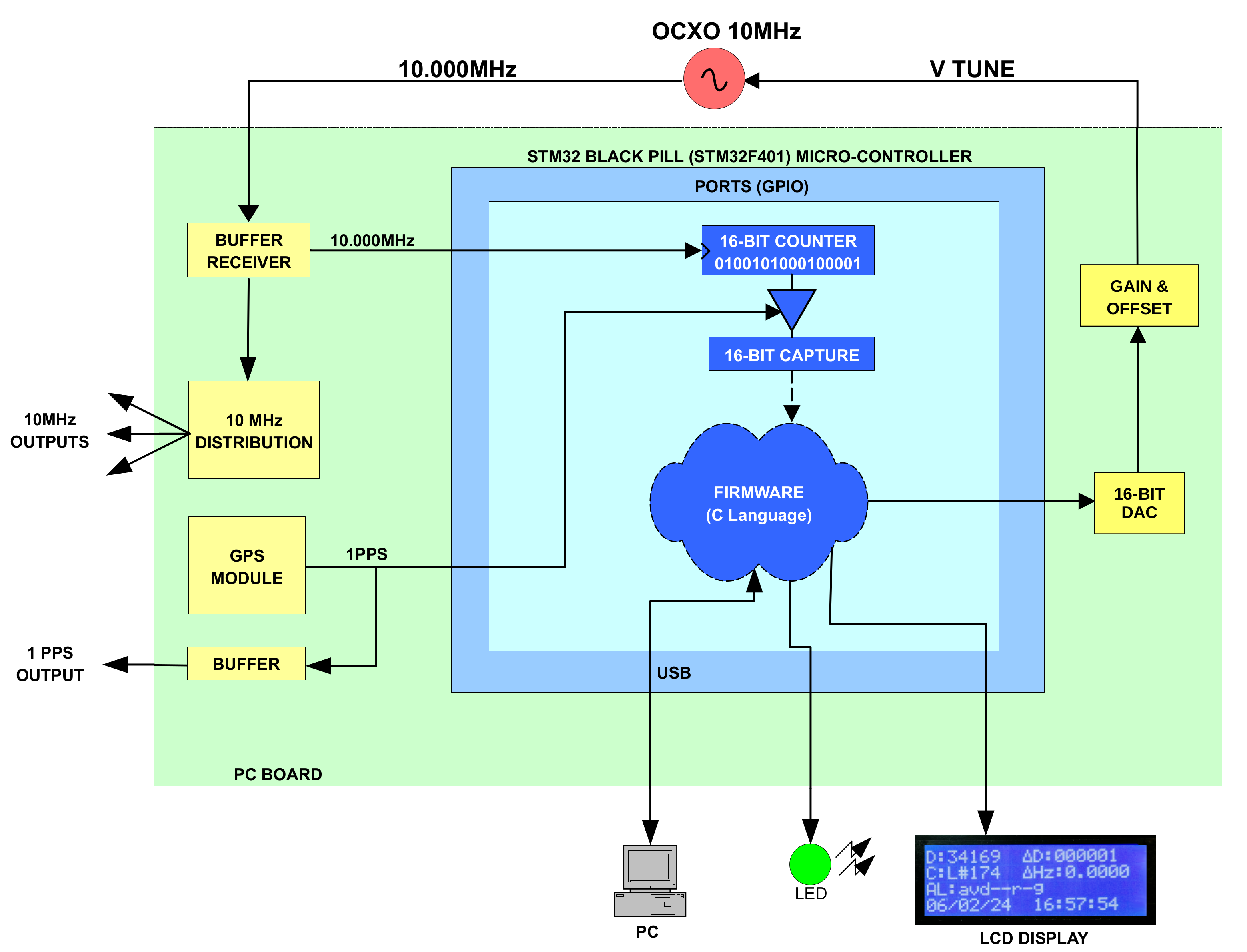
Block diagram of the modernized
version of the VE2ZAZ GPS-Derived Frequency
Standard
This modernized version of
GPS-Derived Frequency Standard offers the
following improvements over the previous
version:
- A
32-bit micro-controller, the STM32 Black
Pill (STM32F401C) or Blue
Pill (STM32F103C) platform
(previously an 8-bit PIC micro-controller),
- A
true 12/14/16-bit
Digital-To-Analog-Converter (DAC) to
generate the OCXO tuning voltage
(previously a PWM output and some low-pass
filtering),
- A
real clock distribution chip with 50
Ohm output impedance to fan out to
the four 10 MHz references (previously a CMOS gate
chip),
- A faster 10MHz signal
receiver/shaper/buffer chip. This provides
a sharper and more accurate 10 MHz
reference into the FLL.
- A 20-character, 4-line LCD
display that provides the essential system
status information (previously
non-existent),
- A buffered 1-PPS output
available for external usage (previously
non-existent)
- Separate
digital and analog +5V rails, for a lower
noise performance (previously a single +5V
rail),
- A firmware developed in C
language on the Arduino IDE environment,
offering easy code change/recompile by the
user (previously coded in unintuitive PIC
assembly language),
- A Proportional-Integral (PI)
FLL loop, yielding a much finer frequency
control and faster convergence (previously a
constant step FLL loop),
- A three-stage FLL
acquisition process: short, medium and long
sampling cycles (previously a two-stage
coarse-fine process). This provides a much
faster convergence towards the ideal 10 MHz
frequency, and a faster recovery from short
or small GPS disturbances.
- A PCB integrating the GPS,
the DAC and even a prototyping area which
can, depending on the model used, hold the
OCXO,
- A native
USB 2.0 serial port on STM32 Black
Pill (the STM32 Blue Pill
requires an external UART-to-USB
converter),
- A comprehensive VT-100 text
console via the USB port for easy
configuration and control of the system
parameters, and for complete status
monitoring (replaces the very basic text
console and the Windows software).
ORIGINAL SYSTEM
DEVELOPMENT
|
In
2022, the author developed and documented
this modernized system in French language,
for the benefit of the French speaking
community. He
created a series of six YouTube videos
documenting the entire development
process and testing of this system. One
would benefit a lot from
watching the videos with the English
subtitles enabled. The video playlist is
accessible by clicking on the thumbnail
to the right.
|
|
Understanding that there was demand for an
English version of this project, the author
has entirely translated to English the
source code, control interface, help screen,
etc. (all variables, constants,
header and comments). It is the English
version that is proposed on this web page.
The
project was designed in
the KiCad electronics
design environment. The
design files (schematics,
PCB, Gerber files) are
packaged in the ZIP file
to the right.
For easy
consultation, a PDF
version of the circuit
schematics is also
available to the right.
The
author is
happy to share
the entire
design with
other users.
Please
understand the
licensing
conditions
before using
it. See the
legal note
below.
Legal
Note
This
hardware design is made
available under the
following license: CC
BY-SA 4.0 (Creative
Commons Attribution-ShareAlike
4.0 International). See this
link for more
detail. In summary:
You are free to:
- Use,
share and adapt the
design, even
commercially,
You must:
- Give
appropriate credit to
the author.
- Distribute
your contributions
under the same
license.
|
|
Here is a list of the required components to put
this project together.
Qty
|
Value |
Description |
Footprint
|
On-Board
Components
|
| 1 |
STM32_BlackPill_BluePill |
STM32_BlackPill
or BluePill board |
TH:
DIP, 40 pins,
0.100” pitch, 0.600” spacing |
| 1 |
100u
16+V |
Polarized
capacitor |
SMD:
6.3x7.7 |
| 2 |
1u
25+V |
Unpolarized
capacitor |
SMD:
1206_3216 |
| 2 |
10u
10+V Tantalum |
Polarized
capacitor |
SMD:
1206_3216 |
| 2 |
100u
25V |
Polarized
capacitor |
SMD:
6.3x7.7 |
| 7 |
100n
25+V |
Unpolarized
capacitor |
SMD:
1206_3216 |
| 1 |
(See
schematics)
Not Installed or
100n 25+V |
Unpolarized
capacitor |
SMD:
1206_3216 |
| 8 |
10n
25+V |
Unpolarized
capacitor |
SMD:
1206_3216 |
| 1 |
BAT54
or
BAT54C or
BAT54S |
Dual
schottky barrier diode |
SMD:
SOT-23 |
| 12 |
Conn_01x02 |
Generic
male connector, single row, 01x02 |
TH:
0.100" Pin Header |
| 1 |
Conn_01x05 |
Generic
male
connector, single row, 01x05 |
TH:
0.100" Pin Header |
| 3 |
Conn_01x04 |
Generic
male
connector, single row, 01x04 |
TH:
0.100" Pin Header |
| 2 |
2N7002 |
0.115A
Id, 60V Vds, N-Channel MOSFET, SOT-23 |
SMD:
SOT-23 |
| 8 |
1K |
Resistor |
SMD:
1206_3216 |
| 1 |
33 |
Resistor |
SMD:
1206_3216 |
| 1 |
4.7K |
Resistor |
SMD:
1206_3216 |
| 1 |
510 |
Resistor |
SMD:
1206_3216 |
| 2 |
10 |
Resistor |
SMD:
1206_3216 |
| 1 |
15K |
Resistor |
SMD:
1206_3216 |
| 1 |
(See
schematics)
Not Installed or
100K |
Resistor |
SMD:
1206_3216 |
| 1 |
(See
schematics)
0 or
62K or
100K |
Resistor |
SMD:
1206_3216 |
| 5 |
51 |
Resistor |
SMD:
1206_3216 |
| 1 |
2K |
Resistor |
SMD:
1206_3216 |
| 2 |
1.8K |
Resistor |
SMD:
1206_3216 |
| 2 |
3.9K |
Resistor |
SMD:
1206_3216 |
| 1 |
3k |
Resistor |
SMD:
1206_3216 |
| 2 |
LM1117-5.0
or equiv. |
800mA
Low-Dropout Linear Regulator, 5.0V fixed
output, TO-220/TO-252/TO-263/SOT-223 |
SMD:
SOT-223-3 |
| 1 |
SN74LV1T34DBV
or
MC74VHC1GT50 |
Single
Power Supply, Single Buffer GATE, CMOS
Logic, Level Shifter, SOT-23-5 |
SMD:
SOT-23-5 |
| 1 |
DAC80501MDGS
or
DAC80501ZDGS or
DAC70501MDGS or
DAC70501ZDGS |
Single
16-bit or 14-bit Digital to Analog
Converter, SPI/I2C Interface, VSSOP-10
package |
SMD:
VSSOP-10 |
| 1 |
OPA2705UA
or
OP279GSZ or
LM6132AIM or
LM6132BIM |
Dual
Op amp, rail-to-rail input/output, Single
supply Vcc up to +15V |
SMD:
SOIC-8 |
| 1 |
DS90C402M |
Dual
LVDS Receiver, >155Mbps, 5V, SOIC-8 |
SMD:
SOIC-8 |
| 1 |
LT6551CMS
or
LT6551IMS |
IC
Video Amp 4-channel Voltage Feedback
10-MSOP |
SMD:
MSOP-10 |
| 2 |
-
|
20-position
single-row female header connector (Used
for STM32 board mounting) |
TH: 0.100"
Female Header |
| Off-Board
Components |
1
|
Morion
MV-89A or
Isotemp OCXO131-100 or equivalent
|
Oven-Controlled
Crystal Oscillator (OCXO). See comments
below.
|
-
|
1
|
ublox
NEO-M8M or
NEO-7M or
NEO-6M
|
Navigation-grade
GPS board with 5 pin interface (1
Pulse-Per-Signal at connector)
|
-
|
1
|
|
Amplified GPS
Antenna
|
-
|
1
|
|
4 Lines by 20
Characters (4x20) LCD display with I2C
add-on board. See picture below. |
-
|
-
|
|
Enclosure,
External power supply,
Additional linear regulator, Various
connectors, Cables and wires, nuts and
bolts,
Power switch, Fuse Holder,
BNC Connectors,
etc.
|
-
|
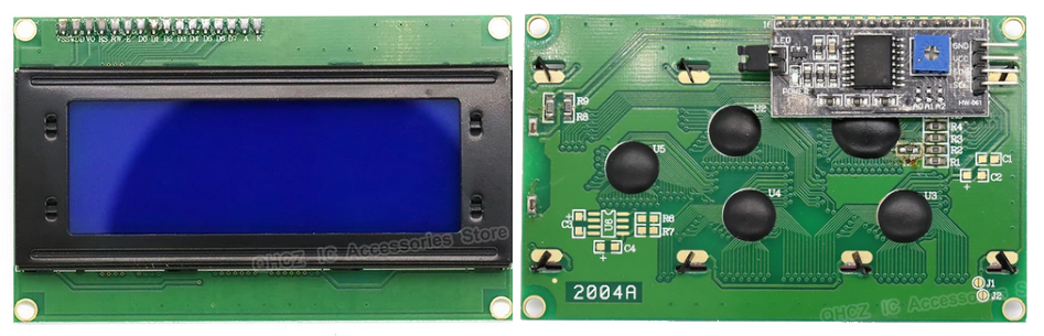
Display
The display is a common 4-line, 20
characters per line, monochrome, backlit
HD44780-compatible LCD unit. This unit
works on a +5V supply, and its signals
have a 5V TTL swing. It is equipped with a
PCF8574-based I2C back-pack
board. The combined display and back-pack
can be purchased from Chinese online
stores for less than $10.
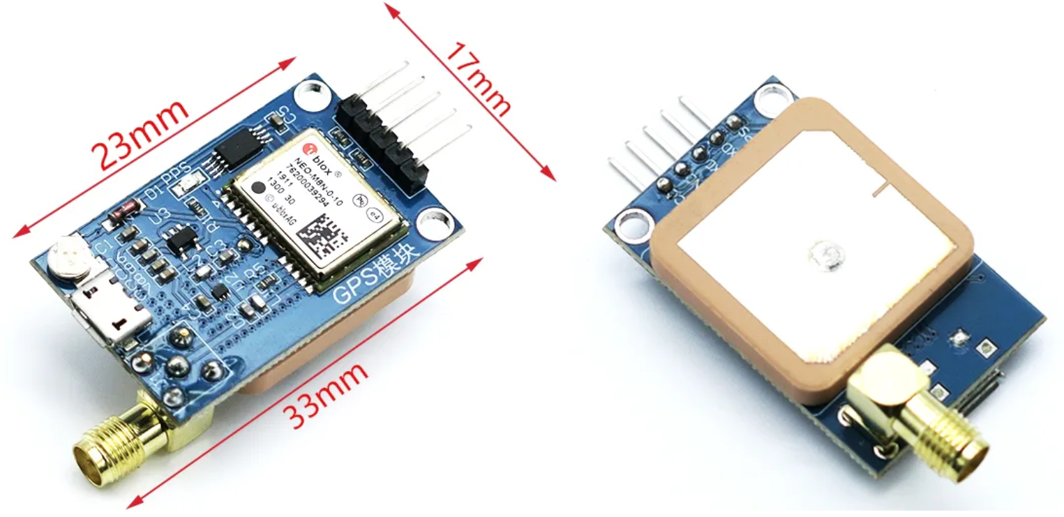
GPS
The GPS used must works
on a +5V supply, and its signals must
have a 3.3V LVTTL swing. It must
have a RF connector for external antenna
support, and provide a 1 Pulse-Per-Second
signal at the connector. Such GPS board
can be purchased from Chinese
online stores for less than $10. The ublox
series of GPS boards is a good choice.
Although using a better timing grade GPS
unit is a sound proposition, any good
navigation grade GPS will do the work just
fine. The reason for this is that the GPS
1 PPS signal gets integrated (averaged)
over a long period by the firmware,
typically a for few hours in duration. The
real gain in system performance is
achieved by this averaging, more than by
the raw GPS performance alone.
Important Note: These GPS boards
typically have an on-board GPS patch
antenna. That antenna is not used when the
GPS is integrated into an enclosure. Thus
that on-board antenna must be
disconnected. More details are provided in
the Assembly section.
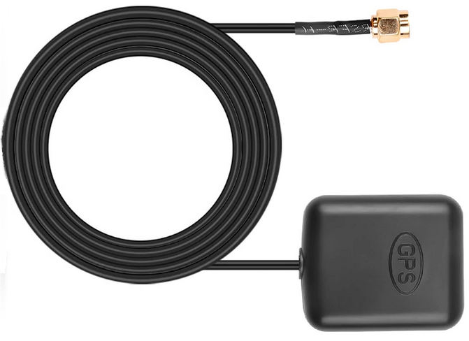
GPS Antenna
A suitable external GPS antenna is
amplified, and has a 3 to 6 meter long
coaxial cable terminated with a male SMA
connector. Such navigation-grade antenna can
be purchased from Chinese
online stores for less than $5.
STM32 Black Pill or
Blue Pill
The
author suggests using the STM32 Black
Pill. There are several
incentives in using the Black Pill
platform, namely cost, availability, CPU
performance, direct USB port vs. requiring
an external Serial-to-USB adapter. Both
the firmware and the system
board can accommodate either a STM32
Black Pill or a STM32 Blue Pill board. By
default, the firmware is configured to run
on a Black Pill platform. When a Blue Pill
is used, a
compiler constant located in
the header of the main C source file
must be commented out (disabled).
The constant to comment out is
"BLACK_PILL_USED".
In addition, the system board must be
configured for either the Black Pill or
the Blue Pill. See the STM32
board type configuration note in
the "ASSEMBLY AND INTEGRATION
NOTES" section for more detail.
|
The
4x20 LCD display with I2C board
A suitable GPS board
A suitable amplified GPS
antenna
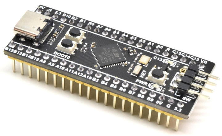
The STM32 Black Pill Board
|
OCXO selection
The 10 MHz oscillator is a key
component in this system. Selecting a good 10
MHz OCXO will improve the performance in terms of
accuracy, stability and phase noise. Understand
that the typical averaging cycle can last a couple
of hours. During that period, the oscillator
frequency must remain as stable as possible,
otherwise the calculated frequency correction will
be meaningless. This is why none of the TCXOs and
VCXOs available on the market are suitable for
this system. As a minimum, a proper GPS-derived
reference oscillator MUST have the following
characteristics:
- It
must be a quartz-based oscillator,
- It must be "ovenized"
(OCXO type),
- It
must be stable in frequency and wave shape,
- It
must have sufficient output amplitude (1 Volt
RMS under load will meet most requirements),
- It
must provide a monotonic output (no ripple or
glitches on the rising/falling edges),
- It
must have a frequency tuning input pin.
The
choice of output wave shape is a criterion to
take into account. Knowing the above,
for the vast majority of clock distribution
applications (feeding test instruments, for
example), a square wave signal is suitable. However
there may be some specific applications (some test
instruments) that require a sine wave signal as
the 10 MHz reference, otherwise the target clock
circuit may misbehave. For these cases, one must
select a sine wave output OCXO. One other benefit
of using a sine wave output is the reduction of RF
pollution caused by the 10 MHz harmonic content.
In the end, the most demanding users call for sine
wave 10 MHz references. It is indeed a wise
choice. Are you one of them?
Like most things in life, you get what you pay
for. New OCXOs are expensive. However one can save
by purchasing a second-hand oscillator. Off-shore
Ebay and AliExpress vendors offer nice units at
relatively low cost (used units from $20 to 100$,
including shipping).
The following units are recommended by the author.
They are listed in order of desirability, from
highest to lowest.
- Morion
MV89: Very desirable (will yield high system
performance). Has a double-oven. +12 VDC
supply, 5 Hz tuning range. Sine wave output.
Simple to integrate into the system. Its cost
has gone up lately, unfortunately.
- Hewlett-Packard
10811 and 10544 series OCXOs: High
performance, 1 Hz tuning range. However are
expensive, are large, require multiple DC
supplies, a negative tuning voltage, and an
adapter PCB. The units in circulation
are getting old and showing some signs of
failure. Note that their frequency vs.
adjustment voltage response has an inverted
behavior. That must be set in the firmware
at compilation time.
- Isotemp
OCXO131-100: Suitable
(will yield slightly degraded system
performance, see comment in the system
performance section), 8 Hz tuning range, 5 VDC
supply, 5V CMOS square wave output.
- Other
Isotemp OCXO131, OCXO134
or OCXO143 series oscillators. Similar
performance as the OCXO131-100.
However some specifications (supply voltage,
output shape, amplitude, tuning range,
stability) may be difficult to determine. With
some research, the user may find a suitable
unit at a very attractive price.
Obviously,
there are many other brands (Ovenaire, Bliley,
Oscilloquartz, Vectron, CTS-Knight, Efratom, etc.)
and models of OCXOs that may be suitable for this
system, however the author has not tested them,
hence cannot make any recommendation. Comparing
specifications between models will show whether an OCXO
is suitable for the task.
DAC Selection
This system is designed to use the Texas
Instrument DACx0501 series of Digital-to-Analog
Converters (DAC). The series offers 16, 14 and 12
bits of resolution, depending on the part
selected. Obviously, the cost of the DAC follows
the resolution. The firmware can accommodate any
of the three resolutions. However, the author
recommends that the 16-bit version (DAC80501)
be selected. A lower number of DAC bits
affects the resolution of the frequency
adjustment, which will degrade system
performance. Considering that the difference in
cost between the different versions of DAC is
only a few dollars, giving up on performance is
not worth the saving, particularly if one spends
much more on a good OCXO, and on the rest of the
system...
Note that the number of bits of the DAC used
must be configured in the system via the control
console.
Also note that the firmware will show DAC values
ranging from 0 to 65535 regardless of the
number of DAC bits used. However when a 14-bit DAC
is used, the DAC value will always
increment/decrement by steps of 4. With a 12-bit
DAC the steps will be of 16 values. This
provides easier firmware compatibility between DAC
versions.
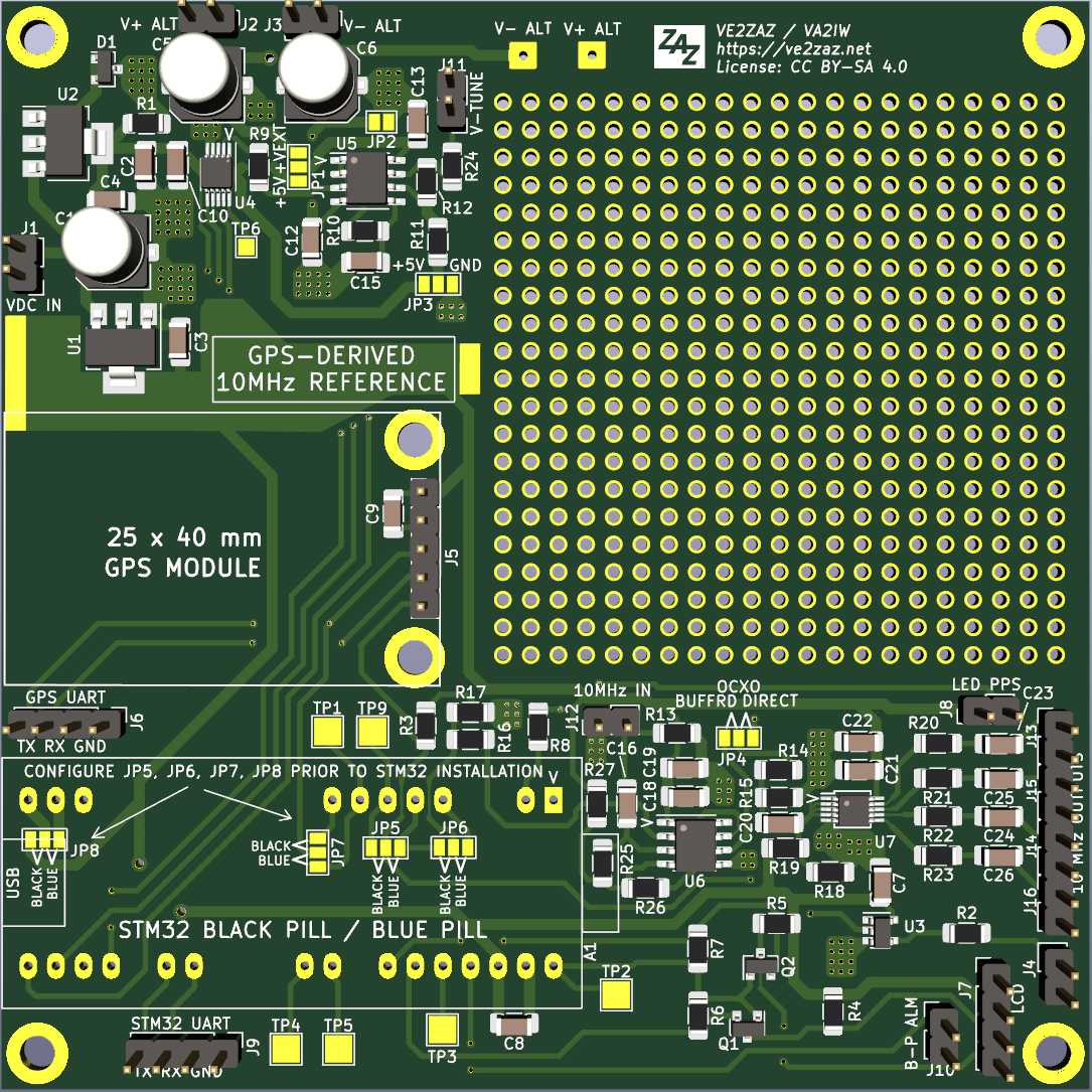
The PCB
has the following
characteristics:
- A
double-sided copper design, however
all components mounted on the top
side,
- 100
mm x 100 mm dimensions, qualifies
for "special price" PCB
manufacturing.
- Recommended
material: FR-4, 1.6 mm (0.062")
thickness.
- Soldermask
and Silkscreen layers provided for
both sides,
- Has
a prototype area for easy circuit
additions,
- Uses
surface-mounted components,
some of which have a very
fine lead pitch,
- Uses fine traces
and vias.
Those
who would like to build this system should
have the PCB made by a reputable PCB
manufacturer (JLCPCB, PCBWay and the
likes). For the order, the
Gerber files need to be
transferred to the manufacturer. The ZIP
file containing the manufacturing files
(Gerber and NC Drill files) is available
to the right.
|
|
Board
Assembly
The system board contains many
surface-mounted components, some
of which have a very fine lead
pitch. This project requires some
SMD soldering equipment and the
skills to operate it. Thus, this
project cannot be put together by
beginners. For them, assistance
from a skilled person is required.
STM32 board
type configuration
Prior
to installing the STM32 board on
the system board, four jumpers
(JP5, JP6, JP7, JP8) must be
configured based on the type of
STM32 board used, either Black
Pill or Blue Pill. These jumpers
are located on the system board,
inside the STM32 board footprint.
See the image to the right for
jumper locations. On each of the
four jumper locations, the gap
between the center pad and the
proper adjacent pad (black or
Blue) must be bridged. A solder
ball between two pads is suitable.
Board
installation
The
STM32 Black Pill or Blue Pill board
has two rows of 20 pins interfacing to
the system board. Although one could
solder the STM32 board directly to the
system board, it is suggested instead
to populate the system board with two
20-position single-row female header
connectors that will mate with the matching
standard single-row
male connectors on the STM32 board.
This will provide the ability to
easily remove and insert the
STM32 board in the future.
GPS
on-board antenna
disconnection
The recommended GPS boards
have an on-board GPS patch
antenna. That antenna will not
be used when the GPS is
integrated into an enclosure.
Thus the on-board antenna must
be disconnected. On the GPS
board, remove the coupling
capacitor (typically C2) that brings
the patch antenna signal to
GPS antenna input.
See picture to the right.
|
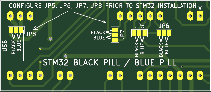
STM32 type
configuration jumper locations
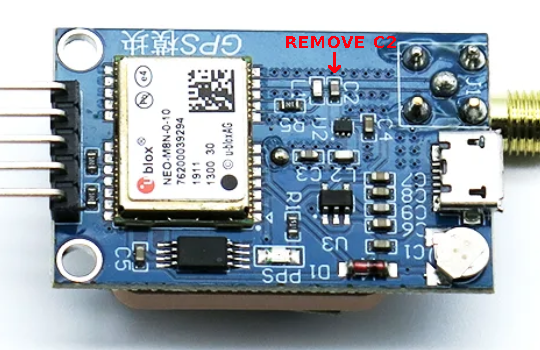
The capacitor to be
removed on the GPS board
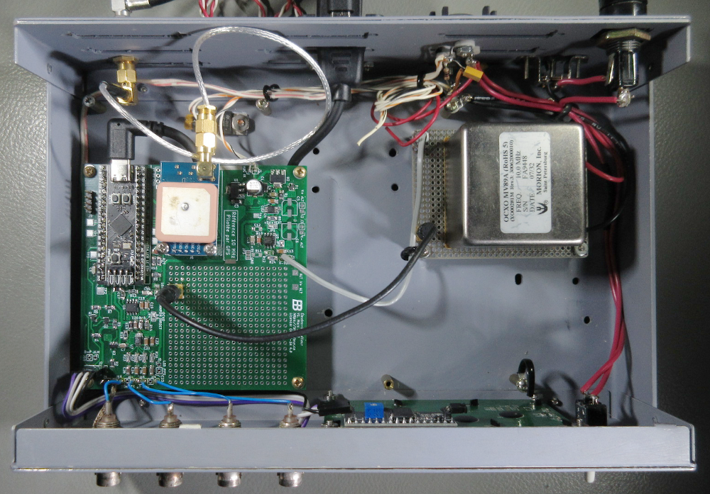
System integration
inside the author's enclosure
|
Power supply
strategy
In
such a high accuracy system, linear DC
supplies should be privileged over switching
supplies. The following power supply
distribution was adopted by the author for
this project. A clean, regulated +12 VDC,
2 Amperes analog supply feeds the entire
project through a 2 Amperes fast-acting
fuse. That +12 VDC is sent to the OCXO, a
Morion MV89A. The +12 VDC rail is
also regulated down to +8 VDC using an LT1084,
TO-3 case, adjustable linear regulator. That
+8 VDC is sent to the project board, which
regulates down to +5 VDC (separate analog and
digital regulators). Typical current of the
system board is 300 milliAmperes. On his
project, the +8 V regulator was already
available in the enclosure, so it was wise to
use it as an intermediate step-down stage to
dissipate some of the heat that would
otherwise have been dissipated by the small +5
V regulators on the system board. Moreover, having a hefty +8V regulator
also allows to feed a separate +5 V
regulator dedicated to the OCXO (in the case
where a +5V OCXO is used), while keeping the
power dissipation from that regulator as low
as possible. Another advantage of
having an additional regulator is the
reduction in noise sent to the system board.
The user will adapt the power distribution
based on OCXO supply requirements. The chosen
OCXO can typically require a +5 or +12 VDC
supply at a current of up to 1.5 Ampere for a
few minutes after power up.
OCXO mounting
Due
to its smaller size, the Isotemp OCXO131
type oscillator can be mounted directly on
the system board, in the prototyping area.
Note that the hole size in that area may be
too small to receive the oscillator pins
directly, so some interfacing plan may have
to be devised. Also note that an external
supply is still required, as the on-board
+5V regulators are not sized for that task.
Other brands and models of OCXOs, due to
their size, may have to be mounted
off-board. A separate prototyping PCB is
suggested as the support for the OCXO. Short
pieces of coaxial cable should be used to
interconnect the oscillator output and the
tuning voltage. See the picture of the
author's system integration inside the
enclosure.
Post-DAC Gain and Offset settings
The voltage
gain and the output offset produced by
the two operational amplifiers that
follow the DAC output must be configured
in hardware. Component U5 contains these
two operational amplifiers. The
Post-DAC Gain and offset values are
determined by the make and model of the
target OCXO. The
user shall consult the OCXO
datasheet to derive its tuning
voltage range. The
implemented gain and offset must produce
a tuning voltage range that matches the
OCXO tuning voltage range.
The Post-DAC gain and offset are set by
configuring resistors, jumpers and
capacitors on the system board during
board assembly, as per the configuration
table on page 4 of the circuit
schematics. The
configuration table is
reproduced here. Notice
that an external supply voltage may be
required for some OCXOs.
OCXO Tuning
Voltage Range |
Post-DAC
Gain |
Post-DAC
Offset (V) |
R11 |
R12 |
C12 |
Jumper JP1
Upper Voltage Rail |
Jumper JP2
Lower Voltage Rail |
Jumper JP2
Offset |
| 0 to +5V |
1.0 |
0.0 |
Not Installed |
0 Ohm |
Not Installed |
Position 1-2 |
Installed |
Not Installed |
| 0 to +8V # |
1.6 |
0.0 |
100K |
62K |
Not Installed |
Position 2-3 |
Installed |
Position 1-2 |
| 0 to +10V # |
2.0 |
0.0 |
100K |
100K |
Not Installed |
Position 2-3 |
Installed |
Position 1-2 |
| -5V to +5V * |
2.0 |
-5.0 |
100K |
100K |
0.1uF |
Position 1-2 |
Not Installed |
Position 2-3 |
*
Configuration used with HP OCXOs
(series 10544 and 10811).
External -5VA_EXT negative
supply required. Voltage must be
equal to
or lower than -5 Volts.
# External +VA_EXT positive
supply required. Voltage must be
equal to or greater than +8
Volts.
The author has found
that a 0 to +5V tuning voltage
(Post DAC gain of 1, offset of
0V) is suitable for his Morion
MV89 and Isotemp OCXO131-100
OCXO units. Other
OCXO makes and
models may
require
different gain
and offset
settings.
10 MHz
Output Wave
Shape
The 10 MHz
reference
outputs can
have the
following wave
shapes
selected in
hardware using
jumper JP4:
- The same wave shape as the
one produced at the OCXO output. For this,
Jumper JP4 must have its positions 1 and 2
shorted together.
- A square wave shape,
regardless of the OCXO
output wave shape. For this,
Jumper JP4 must have its positions 2 and 3
shorted together.
The
firmware load running on the STM32
micro-controller is compiled and
uploaded by the user in the Arduino
IDE programming environment. The IDE
must first be configured to support
the STM32 family of
micro-controllers. Consult the
Internet to find out how to add and
configure the support for the STM32
Black Pill or Blue Pill, as this is
beyond the scope of this web page.
The following Arduino libraries must
be installed in the Library Manager
prior to compiling the code:
- FlashStorage_STM32
- LiquidCrystal_PCF8574
The
latest firmware version is available
on GitHub, at the link provided to
the right.
Legal
Note
This
software
design is made
available
under the
following
license: CC
BY-SA 4.0 (Creative
Commons Attribution-ShareAlike
4.0
International).
See this link for
more detail.
In summary:
You are free
to:
- Use,
share and adapt
the design, even
commercially,
You
must:
- Give
appropriate
credit to the
author.
- Distribute
your
contributions
under the same
license.
Firmware Version History
Version 2 (May
2025): Corrects the
SPI transmission mode to the
DAC80501 chip. Must use mode 2
(falling clock edge latches
the data, high clock level in
idle), as per the DAC
datasheet.
Version 1 (March
2024): Initial English
firmware release.
|
|
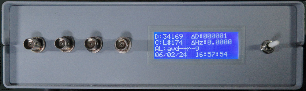
LCD
DISPLAY FIELD DEFINITIONS
|
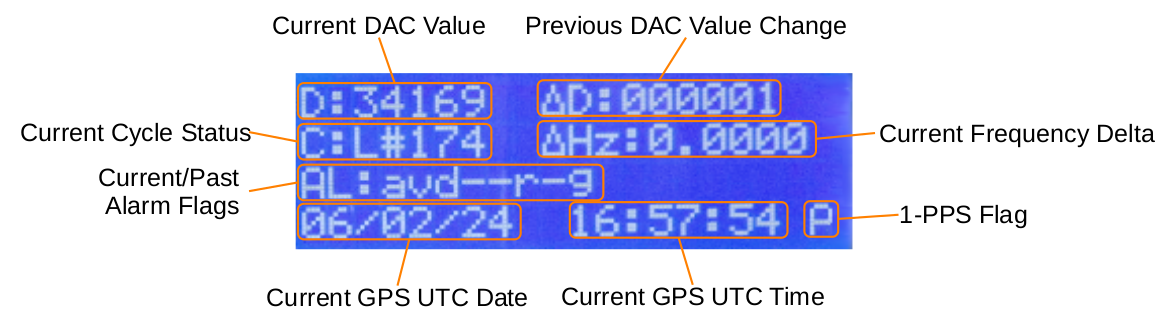
Field
Definitions
- D
- Current DAC value
- ΔD
- Previous cycle DAC value change
- C
- Current Cycle Status:
- Short,
Medium or Long cycle.
- #nnn
is the sample number in the current cycle.
- ΔHz
- Current computed frequency difference from
nominal, in Hz.
- AL
- Alarm field. See types of alarm below.
- An
uppercase character indicate an active alarm
of that type.
- A
lowercase character indicate a previously
active alarm of that type.
- Current
GPS UTC Date, as extracted from the GPS.
- Current
GPS UTC Time, as extracted from the GPS.
- P
(flashing at a 1 Hz rate) - Indicates the
presence of a 1 PPS pulse.
Alarm
types
- A
/ a - In initial acquisition after startup.
- D
/ d - The DAC has reached its minimum or
maximum value.
- F
/ f - The FLL is off.
- P
/ p - GPS PPS signal is missing.
- R
/ r - In long cycle, the sample is
rejected because it is too far away.
- V
/ v - The FLL is unlocked because it is not in
a long cycle.
- O
/ o - The OCXO does not provide a 10 MHz
reference.
- G
/ g - GPS provides invalid data.
GPS
CONFIGURATION AND CONSIDERATIONS
|
2025/02/04:
The following GPS configuration
settings are mandatory in order
for the system to work:
- The
GPS should be configured to output
either the $GPRMC or the $GNRMC
message. All other message types
must be turned off, otherwise
the GPS standard firmware will not
initiate an acquisition. Note: A ublox GPS
receiver will only output $GPRMC
messages when using the GPS
satellites. If other navigation
systems are enabled, the message
header becomes $GNRMC.
- Firmware line 44 must have
the message preamble match the
message sent by the GPS receiver,
either $GPRMC or $GNRMC.
#define
GPRMC_PREAMBLE
"$GPRMC"
or
#define
GPRMC_PREAMBLE
"$GNRMC"
- The GPS serial port bit rate
set in firmware must match the
bit rate of the GPS serial port.
This can be verified/changed at
line 417 of the sketch:
Serial2.begin(9600);
// The “soft” serial port to
receive GPS data
The
following configuration settings are
recommended to extract maximum performance
from the GPS:
- The
GPS should be configured in fixed
position mode,
- The
current LAT and LONG coordinates
should be entered if possible. This
accelerates power up acquisitions.
- The
1-PPS signal should be enabled and
configured to make its rising edge
line up with the time reference. A 10%
duty cycle on the 1-PPS high level
pulse is appropriate.
The user
shall refer to the GPS documentation to
find out how to configure the GPS with the
above settings.
2025/02/04:
Apparently, certain models of ublox GPS
receiver will enter SAFEBOOT mode if the
Timepulse (PPS) pin is held low during
start-up. This affects the M8 models
(there may be others). If you are using
one of these in your build, you must
remove the R3 pull-down resistor on the
VE2ZAZ board.
The system can be
monitored and configured using a serial
console, which is available via a
serial-USB connection sourced from the
STM32 board. When using a Linux-based
computer, the serial port carrying the
console will typically show up as
"/dev/ttyACMxx". On a Windows-based
computer, the serial port will be
identified as COMxx. "xx" is the
port number, and will vary from computer
to computer. Since this is a USB link,
connection parameters (bit rate, parity,
etc) are irrelevant.
Any simple TTY terminal program able to
access the USB ports as serial connections
is suitable for the task. However, a
terminal program supporting the VT-100
protocol will provide additional benefits,
such as non-scrolling status screen and
character highlight. A good, simple
console program for Linux platforms is
Minicom, which is readily available in
most distributions. In Windows, a known
good VT-100 terminal emulation program is
TeraTerm, which is available for free.
Status Reports
The following box shows a typical detailed
status report provided by the serial
console, Such report is printed on the
console screen after every 10-second
sample. In standard TTY
mode, a new status report will make the
information scroll on the screen. In
VT-100 mode, these status fields will
appear static on the screen.
================================================================================
29/02/24-14:31:04-UTC
Alarms:
AL---r-g
Cycle:
Medium
Sample:
10 / 10
Current DAC
value:
34181
Oscillator counter| Nominal
Count:
57599 | 57600
Offset from nominal
count:
-1
Count offset
average:
-0.600000
Offset average
(ppm)
-0.0060
Offset average
(Hz):
-0.060000
Calculated average frequency
of reference (Hz):
9999999.940000
SAMPLING CYCLE COMPLETED
Ajustement made to
DAC:
530
New DAC
value:
34181
Offset calculation (Hz) of PI
loop:
-0.060000
Pause for stabilization...
================================================================================
_1_2_3_4..... |
In addition, there is a condensed status report
available. In this mode, a one-line status
report is printed after every 10-second
sample. Examples of condensed lines are
shown below. Also included are the field
definitions, which can be printed by
typing the DEFIN command (more on the
commands below).
S|29/02/24_20:04:57|al___r_g|34182|L|00002|00720|
00000| 0.00000|________|______
S|29/02/24_20:05:07|al___r_g|34182|L|00003|00720|
00000| 0.00000|________|______
S|29/02/24_20:05:17|al___r_g|34182|L|00004|00720|
00000| 0.00000|________|______
S|29/02/24_20:05:27|al___r_g|34182|L|00005|00720|
00000| 0.00000|________|______
S|29/02/24_20:05:37|al___r_g|34182|L|00006|00720|
00000| 0.00000|________|______
S|29/02/24_20:05:47|al___r_g|34182|L|00007|00720|
00000| 0.00000|________|______
S|
a
|
b |
c |d| e
| f |
g
|
h
|
i |
j |
a: UTC date and time taken
from GPS.
b: Alarm field.
c: Current value of the DAC
(from 0 to 65535) controlling
the OCXO frequency.
d: Current FLL cycle type
(C=Short, M=Medium, L=Long).
e: Sample number in the
current sample cycle.
f: Total number of samples to
collect in the current cycle.
g: Average deviation in
counter pulses from the
nominal value.
h: Average deviation in
counter pulses (g) expressed
in Hertz.
i: Average frequency deviation
of the P-I loop in a long
cycle.
j: DAC change applied at the
end of the current cycle.
|
Configuration
Commands
The system
can be configured using a series of
console commands. Some commands require
one or more parameters to be provided,
otherwise they will be rejected. All
commands must be followed by a LINE FEED.
The following box shows a list of the
available commands and their definition.
The commands can be typed in lowercase or
uppercase. Notice the parameters following
some of the commands. Each parameter has
its range provided within the
<...-...> characters. Parameters
with fixed choices are provided within the
<.../.../...> characters. All
parameters are separated by a space
character.
Commands:
----------
HELP or
?
: This help.
DEFIN
: Help for condensed display
mode fields.
DAC
<0-65535>
: New forced DAC value.
DACBIT
<16/14/12>
: The number of bits used by
the DACx0501.
CYCDUR <1-65535>
<1-65535>
<1-65535> : Number of
samples per short/medium/long
cycles.
CLRALM
: Clears previous alarms shown
in lowercase.
FLL <ON/OFF>
: Enable
FLL.
NPPS
<1-10000>
: Number of PPS per
sample.
PARAM
: List of adjustable
parameters and their current
value.
PI <0-1.0000>
<0-1.0000>
: Constants Kp and Ki of the
P-I loop of t.
RESET
: Restarts the
micro-controller.
REACQ
: Restarts the acquisition
process.
THRES <0-100.0000>
<0-100.0000>
: Thresholds (in Hz) for
switching to medi.
VERBOS
<ON/OFF>
: Detailed display
mode.
VT100 <ON/OFF>
: VT100 option of detailed
display mode.
|
The command definitions
shown above can be printed on screen by
typing either the "?" command or the
"HELP" command.
The current system
parameter values can be printed on the
console with the PARAM command.
Typical parameter data is shown below:
Parameter
Values
----------------
Number of DAC resolution
bits:
16
DAC
value:
34182
Vtune voltage at OCXO
(calculated):
2.59886
FLL
operation:
ON
Number of PPS per
sample:
10
Short cycle duration
(samples):
1
Medium cycle duration
(samples):
10
Long cycle duration
(samples):
720
Medium cycle threshold
(Hz):
0.101000
Long cycle threshold
(Hz):
0.010100
Detailed display
mode:
ON
VT100 detailed display
mode:
ON
PI Loop Index
Kp:
1.00
PI Loop Index
Ki:
0.00
|
Alarms
On both the console and the LCD display,
the alarm field has the same appearance and function:
- There
are 8 positions in the alarm field.
They are: A, L, F, P,
R, V, O, G.
- Each
position shows the status of one
specific alarm.
- Uppercase
letters indicate currently active
alarms,
- Lowercase
letters indicate previous alarms.
- An
underscore or hyphen character
indicates the absence of current or
previous alarm.
- Previous
alarms can be cleared with the
CLRALM command, or by shorting out
the alarm clearing jumper (J10
pins) on the
system board.
The
following box shows the alarm
definitions:
Alarms:
--------
Uppercase letters indicate
currently active
alarms.
Lowercase letters indicate
previous alarms. Can be
cleared with the CLRALM
command.
A /
a
: In initial acquisition after
startup.
L /
l
: The DAC has reached its
minimum or maximum value
(limit).
F /
f
: The FLL is
off.
P /
p
: The GPS PPS signal is
missing.
R /
r
: In long cycle, the sample is
rejected because it is too far
away.
V /
v
: The FLL is unlocked, because
it is not in a long cycle.
O /
o
: The OCXO does not provide a
10 MHz reference.
G /
g
: The GPS provides invalid
data.
|
The alarm definitions shown above can be
printed on screen by typing either the "?"
command or the "HELP" command.
FLL
CONFIGURATION AND
OPERATION
|
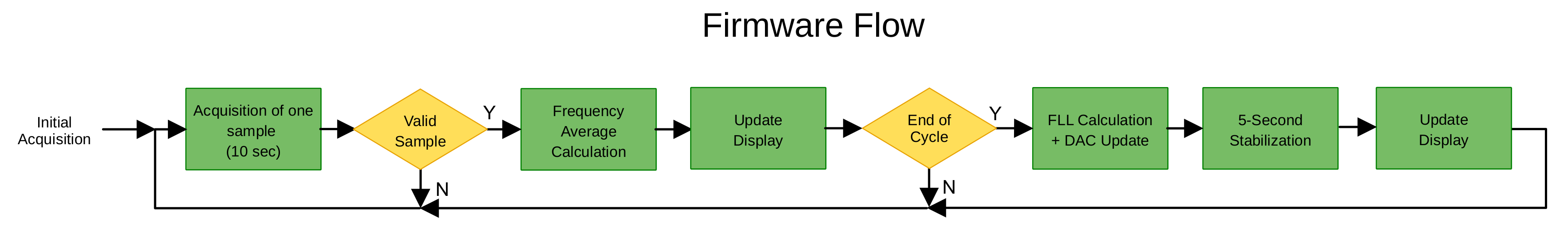
The following diagram
shows the overall FLL process flow.
A description of the FLL behavior follows.
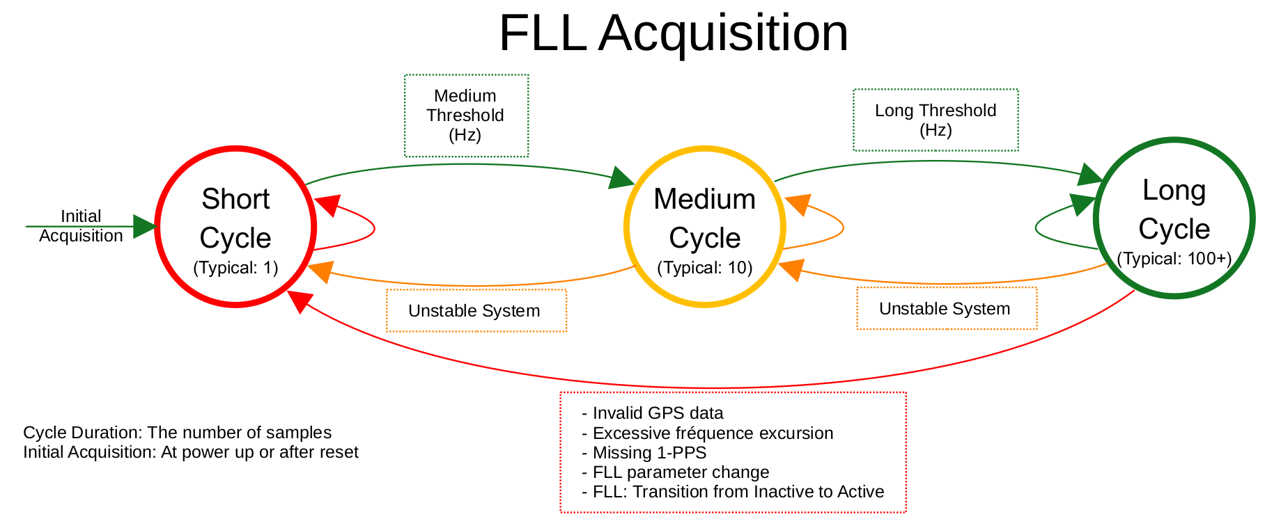
The FLL can
transition between short, medium
and long sampling cycles at the end
of each sampling cycle,
based on the calculated frequency
offset from the nominal 10
MHz target. At
start up, the FLL uses a short cycle
(typically a single sample) to make
coarse frequency corrections. As the
measured OCXO frequency gets closer to
the nominal 10 MHz target, the FLL
transitions to a medium duration
cycle, which produces finer frequency
corrections. On a stable system, the
FLL ultimately
transitions to a long
sampling cycle, which typically lasts
a few hours. The firmware can also
decide to transition back to a shorter
sampling cycle if the latest sample
deviates too much (indicating a
degraded system condition),
or if alarm conditions exist. Note
that cycle
durations and transition thresholds can be
configured by the user at run time
via the serial console.
The P-I
Compensation Loop
The OCXO
frequency adjustment process
implements a
Proportional-Integral (P-I)
compensation loop. As a
result, a frequency
adjustment is
calculated and
applied at the end
of each sampling
cycle via a DAC
value change. Being
a P-I loop, the
applied
DAC
value change
is calculated:
- In
part as a
function of the
latest
measured
frequency
offset
from the target
nominal,
- And
in part by a
longer term
trend of the frequency
offsets.
Note
that the
"differential"
action of a
P-I-D loop is
not
implemented on
this system. A
sample reject
algorithm is
implemented
instead. This
algorithm has
an action
similar to the
differential
action, which
is to reject
grossly
off-frequency
samples (outliers).
Two
coefficients, Kp and Ki, are
used to shift the weight of each
of the two actions, Proportional
and Integral.
These coefficients can be
configured via the serial
console. The
author invites users
to try different
settings and see the
resulting impact on
system behavior and
performance. Nonetheless,
the author has found that the
integral action has
little effect with a
stable OCXO. A
purely proportional loop yields
repeating, fast-converging
and stable results once
the OCXO is fully warmed up and
stabilized.
The following equations
illustrate the proportional and
integral actions in the P-I
loop.
Variables:
OffsetF:
Offset measured in Hz vs. the
nominal target frequency
10.000000000 MHz
OutputF: Value in Hz
used to calculate the DAC
adjustment.
In a P Loop:
OutputF = OffsetF * Kp
This means
the larger the offset is, the
more the DAC value will be
changed.
In a P-I Loop:
OffsetF_accumulation
= OffsetF_accumulation + (OffsetF
*
delta_time)
(accumulated
over 10 cycles)
OutputF
= (OffsetF
* Kp) + (OffsetF_accumulation
* Ki)
This means
the DAC
value change will be
calculated in
part as a function
of how far away from
nominal
the latest measured
frequency is,
and in part by
a longer term
trend of the frequency
offsets.
Loop Index
Conditions:
Kp + Ki = 1 :
Recommended
situation.
Kp + Ki <
1 :
Under-compensated loop. Will
requires more DAC adjustments to
reach the nominal
frequency.
Kp + Ki >
1 :
Over-compensated loop. Not
recommended, will create a
compensation oscillation (the
loop
will
not converge towards the
nominal target
frequency).
Recommended values
(defaults):
Kp = 1 , Ki =
0 : Creates a purely
proportional compensation loop.
Reference material on PID
loops:
PID – Helping
Computers Behave More Like
Humans:
https://spin.atomicobject.com/2016/06/28/intro-pid-control/
Recommended FLL settings
The
author has spent some significant time
analyzing system performance using
various parameter settings, with both
10MHz OCXOs discussed above. Here are
some parameter recommendations for
those of you who don't have the time
or capability to measure frequency
accuracy. Following these
recommendations should allow similarly
built systems to yield good
performance. It must be stated here
that these are only
suggestions. The users shall
see these as a good starting point,
and may find values that better suit
their system setup. It will not damage
anything to play with these
parameters! Worst case, just revert to
these suggested parameters.
| Parameter |
Suggested
Value |
Command
Used |
Note |
| Number of DAC
resolution bits |
16 |
DACBIT 16 |
Must match the DAC
chip resolution populated on the
board. 12 and 14 bit DACs will
degrade performance.
|
| Number of PPS per
sample |
10 |
NPPS 10 |
No real benefit in
changing this value. The internal
counter keeps counting regardless
of the sample duration. In the
end, the samples contribute the
same way to the average
calculation.
Fewer longer samples vs. more
shorter samples.
|
| Short cycle
duration (samples) |
1 |
CYCDUR
1 10 720 |
These
values work well with the MV89
OCXO.
*For the OCXO131-100 OCXO, a one
hour sampling cycle is
recommended. |
| Medium cycle
duration (samples) |
10 |
| Long cycle
duration (samples) |
720
(*360) |
| Medium cycle
threshold (Hz) |
0.101 |
THRES
0.101 0.0101 |
Changing
these values may lead to the FLL
being stuck in shorter cycles, and
not reach the Long cycle, or
transitioning too fast to a longer
cycle.
|
| Long cycle
threshold (Hz) |
0.0101 |
| PI Loop Index Kp |
1.00 |
PI 1
0 |
With
these P-I index values, the FLL
applies frequency corrections in a
proportional fashion, and the
integral contribution is disabled.
The sum of Kp and Ki should never
be greater than 1.00 . See comment
on P-I loop above.
|
| PI Loop Index Ki |
0.00 |
OCXO
CONFIGURATION (IN FIRMWARE)
|
The OCXO
and DAC characteristics must be
captured in the source code header
before compiling the source code for a
given system. This is an important
step to perform in order for the
frequency adjustment to work properly.
The 4 compiler
constants of
interest are:
DAC_VOLTAGE_MIN
DAC_VOLTAGE_MAX
DAC_POST_GAIN
RESPONSE_OCXO_HZ_PER_V
These
constants
are located
near line
number 150 of
the source
code file.
DAC Output
Voltage Limits
First, the minimum and
maximum DAC output voltages must be
measured and entered next to the two
their
respective
constants. The author has already
measured these voltage values
and captured them next to the
appropriate compiler constants
in the source code. It is
expected that these
values will be very
similar from system
to system. They
are:
DAC_VOLTAGE_MIN
0.0123
DAC_VOLTAGE_MAX
4.995
That said, the users may want to
measure these voltages on their
system. The
DAC output
voltage is
probed on
resistor R9. These
measurements can be performed
during the OCXO Frequency
Response measurement below.
Post-DAC Gain
Next, the voltage gain
configured on the operational
amplifiers following the DAC
output must also be captured in
the source code. The Post-DAC
Gain value is dependent on the
make and model of OCXO used. The
implemented gain (and offset)
must produce a tuning voltage
range that matches the OCXO
tuning voltage range.
That gain
is set by
configuring
resistors and
jumpers on the
system board during
board assembly, as
per table
on page 4 of
the circuit
schematics.
A subset of that table is
reproduced here:
OCXO Tuning
Voltage Range |
Post-DAC
Gain |
| 0 to +5V |
1.0 |
| 0 to +8V # |
1.6 |
| 0 to +10V # |
2.0 |
| -5V to +5V * |
2.0 |
The
compiler
constant of
interest is DAC_POST_GAIN.
Refer to item Post-DAC
Gain and Offset Settings
in the
ASSEMBLY AND INTEGRATION NOTES
section to find out what values
to capture in the firmware
source code. As a reminder, the
author has found that a 0 to +5V
tuning voltage is suitable for
his Morion MV89 and Isotemp
OCXO131-100 OCXOs. This
corresponds to a Post-DAC
Gain value of 1.0 .
That value should be
captured next to the
compiler
constant:
DAC_POST_GAIN
1.0
Remember that
other OCXO
makes and
models may
require a
different Post-DAC
Gain
value.
OCXO Frequency
Response
The Frequency
vs. Voltage response (slope) must be
measured, and then entered in the
source code. Optionally, the
minimum and maximum
DAC output voltages
can also be measured
here.
The
compiler constant "RESPONSE_OCXO_HZ_PER_V"
must be
assigned the
proper slope
value. The
number to modify is
located next to the
constant. That value can
be a number with
decimal(s). Note that if
the OCXO lowers its
frequency when its tuning
voltage is increased, the
response value entered
must be negative.
The author has measured the response
values for the two suggested OCXOs.
For these units, simply enter one of
these numbers:
Morion MV89A:
1.489
Isotemp
OCXO131-100:
2.6385
For other OCXOs, the user can execute
the following measurement steps
- Ensure that the system
is stable and that the GPS is
receiving a valid signal.
- Turn off the FLL using
the "FLL OFF"
console command.
- Manually set the DAC
voltage to its maximum using the "DAC 65535"
command.
- Measure the OCXO
frequency with a good frequency
counter, and to the nearest 1/10th
of a Hz. If no frequency counter is
available, use the "Offset average
(Hz):" value provided by status report on the
serial console. Note down the
value.
- Measure the OCXO
tuning voltage at the OCXO. Note
down that value.
- Optionally measure
the DAC output voltage on resistor
R9. This
becomes the DAC_VOLTAGE_MAX constant
value to enter in the source code.
- Manually set the DAC
voltage to its minimum using the "DAC 0"
command.
- Measure and note
down the OCXO frequency.
- Measure
the OCXO tuning voltage at the
OCXO. Note down that value.
- Optionally measure
the DAC output voltage on resistor
R9. This
becomes the DAC_VOLTAGE_MIN constant
value to enter in the source code.
The
RESPONSE_OCXO_HZ_PER_V
value can be
calculated
with:
|
(Step 3-a
Frequency) |
-
|
(Step 4-a
Frequency) |
RESPONSE_OCXO_HZ_PER_V
=
|
----------------------------------------------------------------------
|
|
(Step 3-b
Voltage) |
-
|
(Step 4-b
Voltage) |
Make sure to
recompile the source code with the
updated compiler
constants.
COMMENTS
ON STABILITY AND ACCURACY
|
Since this system combines multiple parts that,
individually, can limit overall system
performance, it is imperative to implement the
best design practices. Examples of good measures
are:
- Selection
of a good, stable OCXO,
- Well
planned DC supply distribution,
- Avoidance
of DC switching converters and supplies,
- Comprehensive
DC supply decoupling,
- Optimization
of wire and cable lengths (shortest possible),
- Use
of coaxial cable wherever noise coupling can
be an issue,
- Optimum
positioning of the GPS antenna,
- Proper
configuration of the GPS parameters,
- Proper
control loop (firmware) parameter
selection.
Due to the numerous
factors that can impact system
behavior, performance is difficult to
guarantee for all systems. Nonetheless, the author has made the following
performance observations on his
system:
- Using a Morion MV89 OCXO,
ublox neo-8 GPS, and for a one-hour
sampling period, his system consistently
produced accuracy figures in the low 10-11's.
- Using an
Isotemp
OCXO131-100 OCXO, ublox neo-8 GPS,
and for a
one-hour sampling period, his system
consistently produced
accuracy figures in the high 10-11's
to the low
10-10's.
- Stability
measurements made by the author over
a one-hour period confirmed a better
medium term stability (less drift)
on the Morion MV89 OCXO
than
on the Isotemp
OCXO131-100 OCXO.
Accuracy and
stability measurements were made by
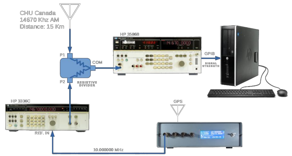
zero-beating a RF generator fed with our
system reference output against the recovered CHU-Canada
shortwave radio station carrier
(guaranteed to be within 5x10-12
of the NRC-Canada cesium fountain
reference, and transmitted 15 km from
the author's lab). The resulting signal
intensity is used to compute the time
interval between two nulls, and thus
derive system accuracy. Examples of
resulting curves are shown below:
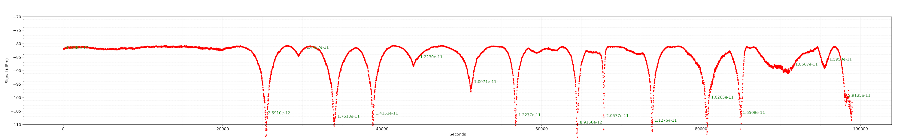
OCXO:
Morion MV89
DAC resolution: 16 bits
Sampling Period: 60
minutes
FLL: Proportional
adjustments
Measurement duration: 27 hours
|
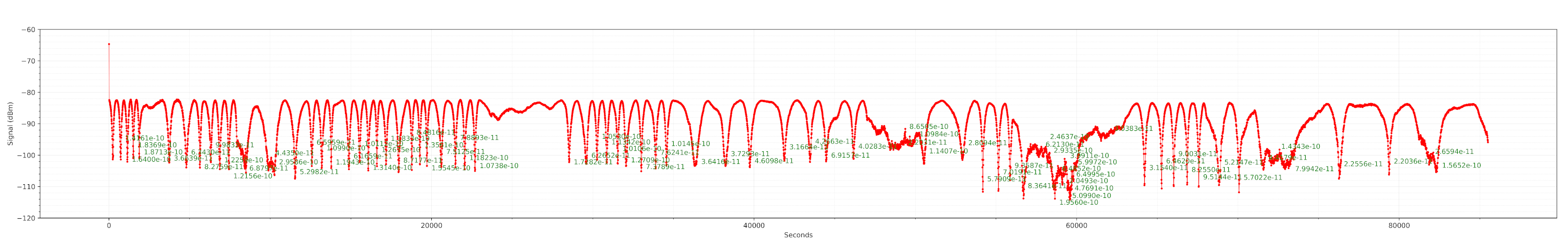
OCXO: Isotemp OCXO131-100
DAC resolution: 14 bits
Sampling Period: 50
minutes
FLL: Proportional
adjustments
Measurement
duration: 24 hours |
Off-Air Measurement Setup
|
As a
complementary exercise, the system
performance was also compared to a Datum
ExacTime 6000 commercial GPS reference
unit. The two systems showed somewhat
different behaviors on a multi-hour
analysis. Nonetheless, as far as
accuracy goes, both systems seemed to
yield similar results, which is a good
sign.
The
author would appreciate reading back from
the experimenters who build this project. This
will allow to improve this page and the
project by providing additional clarification
if necessary. Thanks!
|