|

|
|
A
12 Ghz Prescaler for The HP 5328A Frequency Counter
By: Bertrand
Zauhar, VE2ZAZ
Page last
updated:
21/03/2005
This
page presents an
add-on internal prescaler circuit for the HP 5328A frequency counter.
The Prescaler connects as a front-end to Channel C (520MHz) to provide
a frequency coverage from 100MHz
to more than 12GHz. Actual frequency is displayed,
not a divided ratio.
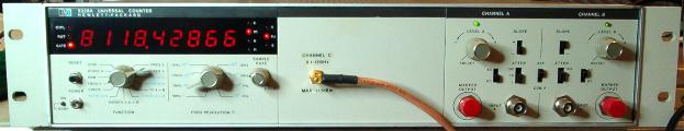
The
HP 5328A
Frequency Counter is a work horse. This is a well engineered 9-digit,
full featured counter with various options such as a DVM, frequency
extension to 520MHz or 1.3 GHz, ovenized TCXO and HP-IB (GPIB).
This counter is readily available on Ebay and in hamfest for less than
$100. These features make it attractive for various modifications.
Adding a microwave prescaler to this counter adds a lot of value to
the instrument. What makes this project feasible is availability of the
Hittite HMC363S8G. This is a
1GHz to 12GHz, divide-by-8 prescaler chip. The component's front end
provides a sensitivity that compares with commercially available
microwave counters. At the other end of the range, the chip can
tolerate input power of +13dBm. Its price is around $8 USD, which is
reasonable even for the hobbyist.
The
idea behind the prescaler implementation is the following: If you
divide down the input signal frequency by a factor N, and you divide
down the counter timebase (reference) frequency by the same ratio N,
the counter
will still read and display the right frequency. In other words, the
counter will count fewer input pulses by a factor N, but the sampling
window is expanded by the same amount N, yielding the same frequency
measurement. The only drawback to this technique is that the sampling
period required to obtain a specified resolution is lengthened by that
same factor N. This does not really constitute a problem in practice
though.
In the case of the HP 5328A, the
following criteria were taken into account when selecting the division
ratio N:
- The maximum frequency expected is 12-15GHz,
this limit
being set by current prescaler chip technology,
- The maximum frequency accepted by the existing
C channel
on the HP 5328A counter is 520MHz,
- The maximum frequency accepted by the A and B
channels is
125MHz,
- The desire to use only one model / one brand
of prescaler
chip to simplify ordering,
- Availability of the prescaler chip via
distributors,
A
compromise value of N=64 was selected. This is obviously achieveable by
using two instances of the same divide-by-8 prescaler chip model.
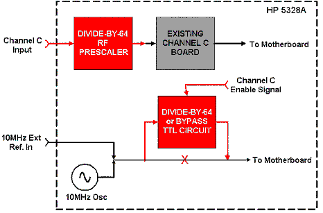
The
figure below shows how my prescaler
is
implemented in the HP 5328A counter.
It
consists of two or modifications:
- The addition of a front end Divide-by-64 RF
prescaler,
- The addition of a 10MHz divide-by-64 TTL
circuit which operates only when
Channel C is selected on the counter.
Note
that
the Prescaler modification
will also work on HP 5328A
counters equipped with the high stability reference TCXO option. As
well, the prescaler boards get installed in the locations normally
equipped by the DVM option boards. Thus, the DVM option is sacrificed
here.
The
Prescaler project is made of two main circuits (PCBs). The figures
below show the two schematic diagrams of these PCBs.
|
The RF Prescaler
Schematic Diagram
A MMIC
amplifier can be added between C4 to C11 to increase sensitivity. If
so, care
must be taken to avoid overloading U1, the first prescaler chip.
|
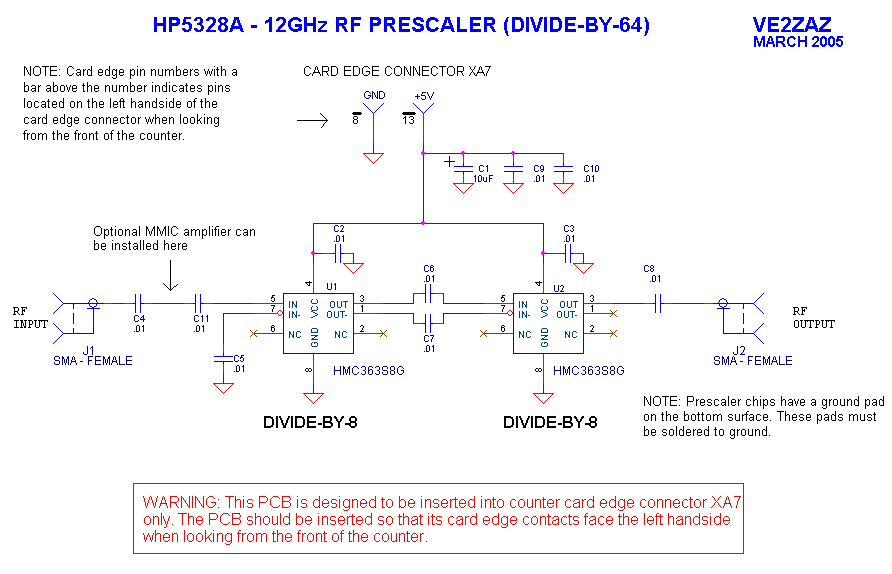
Click
on the
figure to
enlarge it.
|
|
The TTL Divider
Schematic Diagram
JP1, the 4x2
header, can be replaced with a simple wire jumper soldered in place.
|
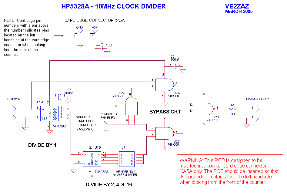
Click
on the
figure to
enlarge |
|
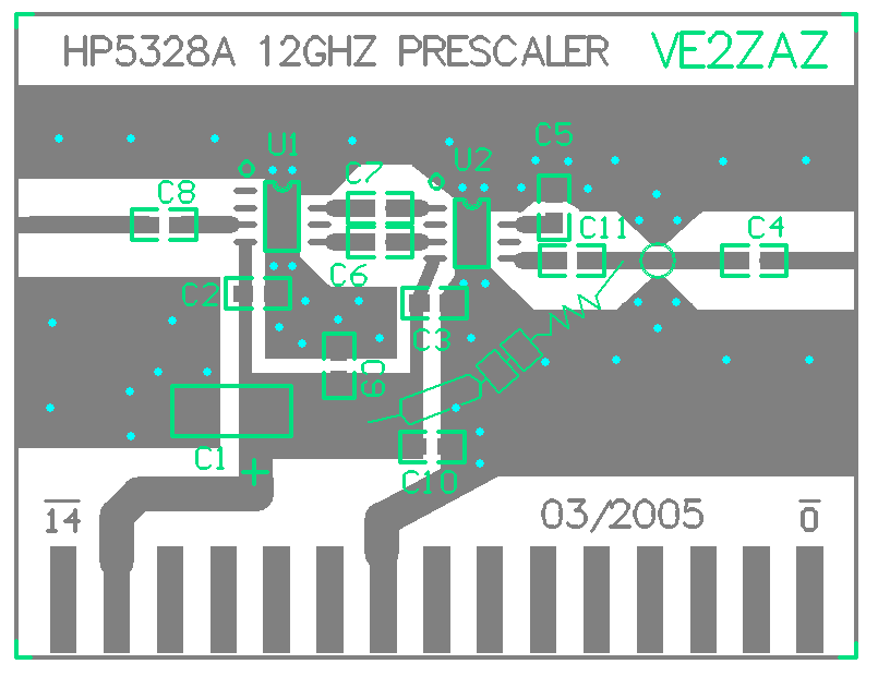
The Prescaler board
layout
- This
PCB is made of double-sided copper clad glass-epoxy materal of 0.031"
thickness. This thickness is important to guarantee a 50 ohm impedance
on the high speed traces.
- The copper pattern resides
on the PCB top side along with the components.
- A solid copper ground plane
must be
present on the bottom side. The ground plane should cover the whole
surface except for the zone underneath the copper fingers at the
bottom. See the picture
below.
- Drilling of holes is
required in marked locations and are only for ground via connections.
- This PCB installs in the
5328A's slot XA7.
|
Click
on the
figure to
enlarge it.
|
|
The TTL Divider
board layout
-
This PCB is
made of single-sided copper clad glass-epoxy materal of
0.062" thickness.
-
This copper
pattern resides on the PCB bottom side. The components are located on
the top side.
-
Drilling of
holes is required to solder the components to the copper pattern.
-
This PCB
installs in the 5328A's slot XA5A.
|
Click
on the
figure to
enlarge it |
|
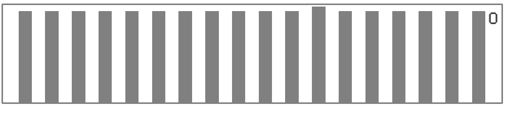
The
Channel C
Enable Signal Pickup board layout
- This PCB
is made of
single-sided copper clad glass-epoxy materal of 0.062"
thickness.
- This PCB
installs in
the
counter's XA5B slot.
It picks up the "Channel C Enable" signal.
|
Click
on the figure to enlarge it
|
If
you wish to make this project, here are the three PCB copper layout
files. These print on Letter-size paper. When printing in full size (no
scaling) the size and proportions should be accurate.
|
ADDITIONAL PCB
ASSEMBLY
INSTRUCTIONS
|
All
Boards
- All three PCB layouts have a
copper outline to mark the edges and ease the cutting process. These
copper outlines should be trimmed off, otherwise short circuits will
occur.
The
Prescaler
board
- This board uses surface-mounted
components. Only experienced
individuals should assemble
it. A
very fine soldering iron tip and a magnifying glass are required.
- Assembly should follow the
following order:
- SMA connectors,
- Ground vias, except for the 4
vias above and below each prescaler chip,
- All capacitors,
- The two prescaler chips (see
note below),
- Remaining ground vias near the
prescaler chips.
- When soldering the SMA connectors
to the pcb edge, ensure you keep the air gap between the connector and
the PCB edge to a minimum. Also, bridge the gap between the bottom
ground plane and the connector ground pins using plenty of solder.
- The two prescaler chips are
modified SOIC-8 package and have a ground pad on their bottom side.
These must be soldered to the PCB ground island first. To do so, apply
a thin amount of solder to the chip and a thin amount of solder to the
copper island. Do not overheat the chip. Drop the chip in place. Heat
up the PCB with the soldering iron as close as possible to the chip
while maintaining the latter in position. Then solder the eight pins.
- Solid pieces of AWG 20
or 22 wire should be inserted in marked locations to act as ground
vias. They should be soldered to both PCB sides and then cut flush with
the surfaces.
The
10MHz
Divider board
- Solder a piece
of wire
between
the Divider board's "Channel C Enable" pad and the longer finger on the
Channel C Enable Signal Pickup PCB.
- The
use of DIP IC sockets is
optional but recommended.
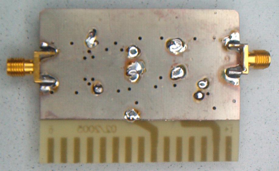
The
Prescaler PCB - Top View
(First Prototype) |

Click
on the
figure to
enlarge it.
|
The
Prescaler PCB - Bottom View
(First
Prototype) |
Click
on the
figure to
enlarge it. |
The
10MHz Divider PCB
and
The Channel C Enable
Signal Pickup PCB
(First Prototypes) |
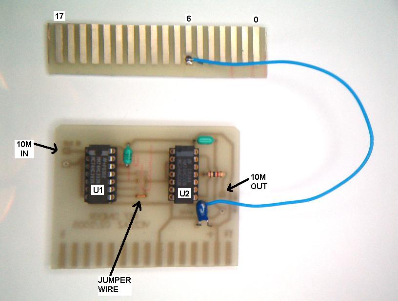
Click
on the
figure to
enlarge it. |
INSTRUCTIONS FOR INTEGRATING INTO HP5328A COUNTER
|
The
HP
5328A counter requires some
minor modifications in order to support the
new 10MHz divider circuit. One small copper trace must be cut to allow
insertion of the divider circuit into the chain. As well two coaxial
cables
are soldered to TTL chip pins. Follow these instructions:
Access
the botton side of the HP 5328A counter motherboard PCB in the 10MHz
reference area (rear-left area when seen from above the counter).
- Cut the trace that links
U16-pin8 to U17-pin13.
|
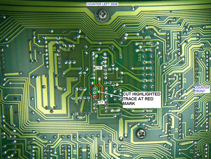
Click
on the
figure to
enlarge it. |
|
Access
the top
side of the HP 5328A
counter motherboard PCB, in the 10MHz reference area (rear-left area
when seen from above the counter). If the counter is equipped with the
HP-IB option, first unscrew the HP-IB board
(including the rear HP-IB connector and
lift the board. Disconnecting the board is not required.
-
Solder a
RG-174 coax cable to U16-pin8. Solder the other end of the coax cable
to the TTL Divider board 10MHz input pad.
-
Solder
another RG-174 coax cable to U17-pin1.
Solder the other end of
the coax cable to the TTL Divider board 10MHz output pad.
-
Only solder
the coax shields at the Divider PCB end. Ensure that the shields are
insulated at the counter's end.
-
If
necessary, re-install the HP-IB option board.
|

Click
on the
figure to
enlarge it. |
Now
is the
time to install the two PCBs
inside the counter. The prescaler fits in the locations where the DVM
options normally reside. If the counter is equipped with a DVM option,
you must first remove the PCBs that equip the left handside DVM option
slots, namely XA5A,XA5B,XA6 and XA7, and associated faceplate.
- Insert
the TTL
Divider
board in slot XA5A as shown in the picture. Components must face the
right handside when looking from the front of the counter.
- Insert
the Channel C Enable
signal pickup PCB in slot XA5B as shown in the picture. The copper
fingers
on the PCB must face the right handside of the counter when looking
from the front of the counter and finger 0 should be closest to the
front of the counter. The wire should come out near the top edge
of the PCB.
|
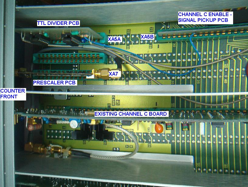
Click
on the figure to enlarge it.
|
- Insert
the Prescaler
board
in slot
XA7 as shown in the picture. Components and copper traces must face the
left handside when looking from the front of the counter. Since the
PCB in only 0.031" thick (half the thickness of a typical PCB, you must
also insert an insulated
shim of equivalent thickness on the back of the PCB finger area. A
piece of plastic or PCB material (copper removed) can be used.
- Connect
the Prescaler
RF
output SMA to the Existing Channel C input cable using a SMA-SMB coax
cable/adapter combination.
- Hook up the Prescaler Input
SMA to a RF connector previously installed on the faceplate.
|
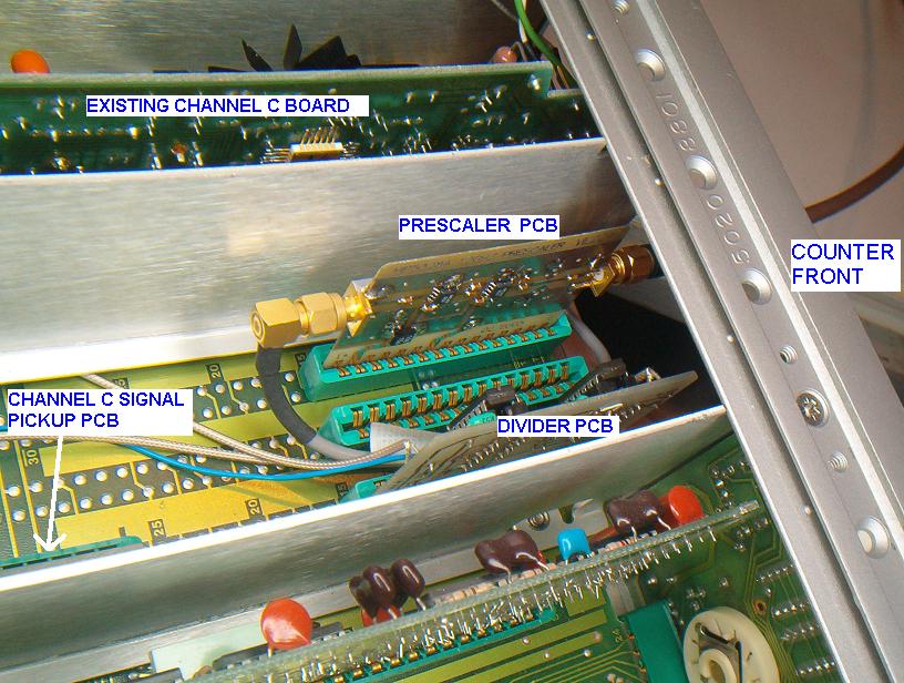
Click
on the
figure to
enlarge it.
|
|
OPERATION AND
PERFORMANCE
|
If
everything visually checks OK ,
apply power to the counter. When selecting channel C with no signal
applied, you will see an erratic frequency display. This is
normal since the noise generated by the prescaler is enough to trigger
the Channel C gate. Apply a 0dBm, 1GHz RF signal. The counter
should display an accurate and consistent frequency. Try different
frequency and amplitude signals to verify proper opration.
Switch back to Channel A and apply a signal, for example 100MHz, to
input A. Verify proper operation.
The following plot shows the
operational range of the finished Prescaler. Between 1GHz and 12GHz,
sensitivity is better than -20dBm (22mV). The high end limit is set by
the maximum input tolerated by the prescaler MMIC chip, which is
+13dBm. The prescaler is usable up to 15GHz with reduced operational
amplitude range. This performance compares favorably with
commercially-made
units.
The
HP 5328A Prescaler Operational Range
|

Click
on the
figure to
enlarge it.
|
Table
1: 12GHz
Prescaler board Parts List (Version 1)
| Qty |
Designation |
Description |
| 1 |
C1 |
10uF,
10V surface-mounted Tantalum capacitor
|
| 10 |
C2-C11 |
10nF,
chip 0805 size capacitor
|
2
|
J1,
J2
|
SMA
connector,
PCB mount female.
|
| 2 |
U1,
U2
|
HMC363S8G,
12GHz,
Divide-by-8 MMIC prescaler chip, modified SO-8 package. Available from
Future-Active, (http://www.future-active.com)
|
| PCB
material, double-sided
copper clad glass-epoxy materal of 0.031" thickness. |
Table
2:
10MHz
Divider board Part List (Version 1)
| Qty |
Designation |
Description |
| 1 |
C1 |
10uF,
10V or higher , Electrolytic capacitor |
2
|
C2,
C3 |
100nF, 10V or higher, Ceramic capacitor |
1
|
JP1
|
Header
2
x 4, 0.1 inch pitch, OR short piece of wire
|
1
|
R1 |
33
ohm
1/4W axial resitor
|
| 1 |
U1 |
74HC393,
Dual 4 bit counter chip
|
1
|
U2 |
74HC00,
Quad NAND gate chip
|
2
|
-
|
DIP-14
pins
sockets (optional)
|
3
Feet of RG-174 coaxial cable
|
8
inches of hook up wire
|
| PCB
material, single-sided
copper clad glass-epoxy materal of 0.062" thickness. |
|